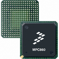
MC68360VR25VL Freescale Semiconductor, MC68360VR25VL Datasheet - Page 513

MC68360VR25VL
Manufacturer Part Number
MC68360VR25VL
Description
IC MPU QUICC 25MHZ 357-PBGA
Manufacturer
Freescale Semiconductor
Datasheets
1.MC68EN360VR25L.pdf
(14 pages)
2.MC68EN360VR25L.pdf
(2 pages)
3.MC68360AI25L.pdf
(962 pages)
Specifications of MC68360VR25VL
Processor Type
M683xx 32-Bit
Speed
25MHz
Voltage
3.3V
Mounting Type
Surface Mount
Package / Case
357-PBGA
Family Name
M68000
Device Core
ColdFire
Device Core Size
32b
Frequency (max)
25MHz
Instruction Set Architecture
RISC
Operating Supply Voltage (max)
3.3V
Operating Supply Voltage (min)
2.7V
Operating Temp Range
0C to 70C
Operating Temperature Classification
Commercial
Mounting
Surface Mount
Pin Count
357
Package Type
BGA
Lead Free Status / RoHS Status
Lead free / RoHS Compliant
Features
-
Lead Free Status / Rohs Status
Compliant
Available stocks
Company
Part Number
Manufacturer
Quantity
Price
Company:
Part Number:
MC68360VR25VL
Manufacturer:
Exar
Quantity:
160
Company:
Part Number:
MC68360VR25VL
Manufacturer:
Freescale Semiconductor
Quantity:
10 000
Company:
Part Number:
MC68360VR25VLR2
Manufacturer:
Freescale Semiconductor
Quantity:
10 000
- Current page: 513 of 962
- Download datasheet (4Mb)
7.10.17.15 SCC HDLC EXAMPLE #2. •The following is an initialization sequence for an
7.10.18 HDLC Bus Controller
HDLC bus is an enhancement of HDLC that allows an HDLC-based LAN and other HDLC
point-to-multipoint configurations to be easily implemented. Most versions of HDLC-based
controllers only provide point-to-point communications.
26. Set the PSMR4 to $0000 to configure one opening and one closing flag, 16-bit
27. Write $00000030 to GSMR_L4 to enable the SCC4 transmitter and receiver. This
1. Follow all the steps in the HDLC Example #1, until the step where the GSMR is initial-
2. Write $00000000 to GSMR_H4 to enable normal behavior of the CTS and CD pins,
3. Write $004AA400 to GSMR_L4 to configure carrier sense always active, a 16-bit pre-
4. Set the PSMR4 to $0000 to configure one opening and one closing flag, 16-bit CCITT-
5. Write $004AA430 to GSMR_L4 to enable the SCC4 transmitter and receiver. This ad-
SCC HDLC channel that uses the DPLL in a Manchester encoding. The user provides
a clock that is 16x the desired bit rate, on the CLK7 pin. CLK7 is then connected to the
HDLC transmitter and receiver. (A baud rate generator could have been used instead,
if desired). SCC4 is used. The HDLC controller is configured with the RTS4, CTS4, and
CD4 pins active.
is desired, set the RINV and TINV bits.
CCITT-CRC, and prevention of multiple frames in the FIFO.
additional write ensures that the ENT and ENR bits will be enabled last.
ized.
and idles between frames (as opposed to flags).
amble of "01" pattern, 16x operation of the DPLL for the receiver and transmitter,
Manchester encoding for the receiver and transmitter, the CTS and CD pins to auto-
matically control transmission and reception (DIAG bits), and the HDLC mode. Notice
that the transmitter (ENT) and receiver (ENR) have not been enabled yet.
CRC, and not allowing multiple frames in the FIFO.
ditional write ensures that the ENT and ENR bits will be enabled last.
After 5 bytes and CRC have been transmitted, the Tx BD is
closed. Additionally, the receive buffer is closed after a frame is
received. Any additional receive data beyond 256 bytes or a sin-
gle frame will cause a busy (out-of-buffers) condition since only
one Rx BD was prepared.
After the preamble and 5 bytes have been transmitted, the Tx
BD is closed. Additionally, the receive buffer is closed after 16
bytes have been received. Any additional receive data beyond
16 bytes will cause a busy (out-of-buffers) condition since only
one Rx BD was prepared.
Freescale Semiconductor, Inc.
For More Information On This Product,
MC68360 USER’S MANUAL
Go to: www.freescale.com
NOTE
NOTE
Serial Communication Controllers (SCCs)
Related parts for MC68360VR25VL
Image
Part Number
Description
Manufacturer
Datasheet
Request
R
Part Number:
Description:
Manufacturer:
Freescale Semiconductor, Inc
Datasheet:

Part Number:
Description:
MC68360 MC68360 Multiple Ethernet Channels on the QUICC
Manufacturer:
Motorola / Freescale Semiconductor

Part Number:
Description:
MC68360 Implementing an 8 bit Eprom for an MC68EC040-MC68360 System
Manufacturer:
Motorola / Freescale Semiconductor

Part Number:
Description:
MC68360 Interfacing the MC68060 to the MC68360
Manufacturer:
Motorola / Freescale Semiconductor

Part Number:
Description:
MC68360 MC68360 RAM Microcode Package Option Overview
Manufacturer:
Motorola / Freescale Semiconductor

Part Number:
Description:
MC68360 MC68360 CPM-CPU Interaction
Manufacturer:
Motorola / Freescale Semiconductor

Part Number:
Description:
MC68360 Interfacing SDRAM to the MC68360 QUICC Device
Manufacturer:
Motorola / Freescale Semiconductor

Part Number:
Description:
MC68360 Interfacing the QUICC to a MCM516400 (4Mx4 10-12 column-row) DRAM
Manufacturer:
Motorola / Freescale Semiconductor

Part Number:
Description:
MC68360 Interfacing the 68360 (QUICC) to T1-E1 Systems
Manufacturer:
Motorola / Freescale Semiconductor

Part Number:
Description:
MC68360 Multiple QUICC Design Concept
Manufacturer:
Motorola / Freescale Semiconductor
Part Number:
Description:
Manufacturer:
Freescale Semiconductor, Inc
Datasheet:
Part Number:
Description:
Manufacturer:
Freescale Semiconductor, Inc
Datasheet:
Part Number:
Description:
Manufacturer:
Freescale Semiconductor, Inc
Datasheet:
Part Number:
Description:
Manufacturer:
Freescale Semiconductor, Inc
Datasheet:
Part Number:
Description:
Manufacturer:
Freescale Semiconductor, Inc
Datasheet:


