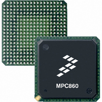
MC68360VR25VL Freescale Semiconductor, MC68360VR25VL Datasheet - Page 733

MC68360VR25VL
Manufacturer Part Number
MC68360VR25VL
Description
IC MPU QUICC 25MHZ 357-PBGA
Manufacturer
Freescale Semiconductor
Datasheets
1.MC68EN360VR25L.pdf
(14 pages)
2.MC68EN360VR25L.pdf
(2 pages)
3.MC68360AI25L.pdf
(962 pages)
Specifications of MC68360VR25VL
Processor Type
M683xx 32-Bit
Speed
25MHz
Voltage
3.3V
Mounting Type
Surface Mount
Package / Case
357-PBGA
Family Name
M68000
Device Core
ColdFire
Device Core Size
32b
Frequency (max)
25MHz
Instruction Set Architecture
RISC
Operating Supply Voltage (max)
3.3V
Operating Supply Voltage (min)
2.7V
Operating Temp Range
0C to 70C
Operating Temperature Classification
Commercial
Mounting
Surface Mount
Pin Count
357
Package Type
BGA
Lead Free Status / RoHS Status
Lead free / RoHS Compliant
Features
-
Lead Free Status / Rohs Status
Compliant
Available stocks
Company
Part Number
Manufacturer
Quantity
Price
Company:
Part Number:
MC68360VR25VL
Manufacturer:
Exar
Quantity:
160
Company:
Part Number:
MC68360VR25VL
Manufacturer:
Freescale Semiconductor
Quantity:
10 000
Company:
Part Number:
MC68360VR25VLR2
Manufacturer:
Freescale Semiconductor
Quantity:
10 000
- Current page: 733 of 962
- Download datasheet (4Mb)
9.2 HOW TO TAKE A QUICC SOFTWARE TEST-DRIVE
At first glance, the QUICC has so many features that the proper initialization sequence may
not be immediately obvious. The following paragraphs address the issue by showing the
proper initialization sequence to use when configuring the QUICC in a system after a power-
up reset.
Included is a step-by-step sequence that will allow the user to use and learn each feature of
the QUICC in a methodical way. The sequence is applicable whether the QUICC is in normal
mode (CPU32+ enabled) or slave mode (CPU32+ disabled). Although the sequence is
designed as a first-time test-drive of the QUICC, it is also useful as a general pattern for an
overall QUICC initialization.
Detailed information of a specific QUICC hardware configuration and the actual values that
should be written to registers may be found in 9.1 Minimum System Configuration and 9.4
Using the QUICC MC68040 Companion Mode . Additionally, many examples of initializing
certain peripherals are contained elsewhere in this manual where that peripheral is
described.
Step 1: Decide on Reset Stack Pointer and Initial Program Counter
CS0 will function after reset and allow code execution from the boot EPROM-type device.
The stack pointer and the reset vector will be read from the first locations of the EPROM,
and the program will execute from EPROM at the initial program counter address offset in
the EPROM. Although the stack pointer is initialized, it is not ready to be used because it
does not yet point to RAM.
Step 2: Stay in Supervisor Mode
After a reset, M68000 family CPUs are in supervisor mode. Program accesses are issued
with the supervisor program function code, and data accesses are issued with the supervi-
sor data function code. These function codes are required for some of the operations that
• To configure the QUICC for 16-bit data bus mode, the system RESET signal should be
• All port sizes should be configured to either 8 or 16 bits. The DRAM port size must be
• Only the D31–D16 pins should be connected to the system bus. Only PRTY0 and
• Only the upper word of the static RAM array should be used. The CS3 line should be
• The DRAM SIMM should be replaced with a 16- or 18-bit-wide version. The RAS1 line
• Only the upper 256K
connected to the PRTY3 pin. In 16-bit data bus mode, the PRTY2 and PRTY3 pins are
not used.
16-bits if internal address multiplexing is used.
PRTY1 should be used. The unused data and parity pins should be pulled high or low
through a resistor to save power and to avoid floating inputs.
programmed to respond to a 64-Kbyte address space.
should be programmed to respond to a 2-Mbyte address space.
programmed to respond to a 512-Kbyte address space.
Freescale Semiconductor, Inc.
For More Information On This Product,
16 bit DRAM device should be used. The RAS1 line should be
MC68360 USER’S MANUAL
Go to: www.freescale.com
Applications
Related parts for MC68360VR25VL
Image
Part Number
Description
Manufacturer
Datasheet
Request
R
Part Number:
Description:
Manufacturer:
Freescale Semiconductor, Inc
Datasheet:

Part Number:
Description:
MC68360 MC68360 Multiple Ethernet Channels on the QUICC
Manufacturer:
Motorola / Freescale Semiconductor

Part Number:
Description:
MC68360 Implementing an 8 bit Eprom for an MC68EC040-MC68360 System
Manufacturer:
Motorola / Freescale Semiconductor

Part Number:
Description:
MC68360 Interfacing the MC68060 to the MC68360
Manufacturer:
Motorola / Freescale Semiconductor

Part Number:
Description:
MC68360 MC68360 RAM Microcode Package Option Overview
Manufacturer:
Motorola / Freescale Semiconductor

Part Number:
Description:
MC68360 MC68360 CPM-CPU Interaction
Manufacturer:
Motorola / Freescale Semiconductor

Part Number:
Description:
MC68360 Interfacing SDRAM to the MC68360 QUICC Device
Manufacturer:
Motorola / Freescale Semiconductor

Part Number:
Description:
MC68360 Interfacing the QUICC to a MCM516400 (4Mx4 10-12 column-row) DRAM
Manufacturer:
Motorola / Freescale Semiconductor

Part Number:
Description:
MC68360 Interfacing the 68360 (QUICC) to T1-E1 Systems
Manufacturer:
Motorola / Freescale Semiconductor

Part Number:
Description:
MC68360 Multiple QUICC Design Concept
Manufacturer:
Motorola / Freescale Semiconductor
Part Number:
Description:
Manufacturer:
Freescale Semiconductor, Inc
Datasheet:
Part Number:
Description:
Manufacturer:
Freescale Semiconductor, Inc
Datasheet:
Part Number:
Description:
Manufacturer:
Freescale Semiconductor, Inc
Datasheet:
Part Number:
Description:
Manufacturer:
Freescale Semiconductor, Inc
Datasheet:
Part Number:
Description:
Manufacturer:
Freescale Semiconductor, Inc
Datasheet:


