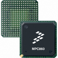
MC68360VR25VL Freescale Semiconductor, MC68360VR25VL Datasheet - Page 690

MC68360VR25VL
Manufacturer Part Number
MC68360VR25VL
Description
IC MPU QUICC 25MHZ 357-PBGA
Manufacturer
Freescale Semiconductor
Datasheets
1.MC68EN360VR25L.pdf
(14 pages)
2.MC68EN360VR25L.pdf
(2 pages)
3.MC68360AI25L.pdf
(962 pages)
Specifications of MC68360VR25VL
Processor Type
M683xx 32-Bit
Speed
25MHz
Voltage
3.3V
Mounting Type
Surface Mount
Package / Case
357-PBGA
Family Name
M68000
Device Core
ColdFire
Device Core Size
32b
Frequency (max)
25MHz
Instruction Set Architecture
RISC
Operating Supply Voltage (max)
3.3V
Operating Supply Voltage (min)
2.7V
Operating Temp Range
0C to 70C
Operating Temperature Classification
Commercial
Mounting
Surface Mount
Pin Count
357
Package Type
BGA
Lead Free Status / RoHS Status
Lead free / RoHS Compliant
Features
-
Lead Free Status / Rohs Status
Compliant
Available stocks
Company
Part Number
Manufacturer
Quantity
Price
Company:
Part Number:
MC68360VR25VL
Manufacturer:
Exar
Quantity:
160
Company:
Part Number:
MC68360VR25VL
Manufacturer:
Freescale Semiconductor
Quantity:
10 000
Company:
Part Number:
MC68360VR25VLR2
Manufacturer:
Freescale Semiconductor
Quantity:
10 000
- Current page: 690 of 962
- Download datasheet (4Mb)
Parallel I/O Ports
All PCDIR bits and PCPAR bits are cleared on total system reset, configuring all port pins
as general-purpose input pins. Note that the global CIMR is also cleared on total system
reset so that, if any PCIO pin is left floating, it will not cause a false interrupt.
If a port C pin is selected as a general-purpose I/O pin, it may be accessed through the port
C data register (PCDAT). Data written to the PCDAT is stored in an output latch. If a port C
pin is configured as an output, the output latch data is gated onto the port pin. In this case,
when PCDAT is read,the port pin itself is read. If a port C pin is configured as an input, data
written to PCDAT is still stored in the output latch but is prevented from reaching the port
pin. In this case, when PCDAT is read, the state of the port pin is read.
To configure a port C pin an a general-purpose output pin, use the following steps. Note that
when the pin is configured as an output, port C interrupts are not possible.
To configure a port C pin as a general-purpose input pin that does not generate an interrupt,
use the following steps:
When a port C pin is configured as a general-purpose I/O input, a change according to the
port C interrupt register (PCINT) will cause an interrupt request signal to be sent to the CPM
interrupt controller. Each port C line can be programmed to assert an interrupt request upon
a high-to-low change or any change. Each port C line asserts a unique interrupt request to
the CPM interrupt pending register and has a different internal interrupt priority level within
the CPM interrupt controller. See 7.15 CPM Interrupt Controller (CPIC) for more details.
Each request can be masked independently in the CPM interrupt mask register.
To configure a port C pin an a general-purpose input pin that generates an interrupt, use the
following steps:
7-366
1. Write the corresponding PCPAR bit with a zero.
2. Write the corresponding PCDIR bit with a one.
3. Write the corresponding PCSO bit with a zero (for the sake of clarity).
4. The corresponding PCINT bit is a don’t care.
5. Write the pin value using the PCDAT.
1. Write the corresponding PCPAR bit with a zero.
2. Write the corresponding PCDIR bit with a zero.
3. Write the corresponding PCSO bit with a zero.
4. The corresponding PCINT bit is a don’t care.
5. Write the corresponding CIMR bit with a zero to prevent interrupts from being gener-
6. Read the pin value using the PCDAT.
1. Write the corresponding PCPAR bit with a zero.
2. Write the corresponding PCDIR bit with a zero.
3. Write the corresponding PCSO bit with a zero.
ated to the CPU32+ core.
Freescale Semiconductor, Inc.
For More Information On This Product,
MC68360 USER’S MANUAL
Go to: www.freescale.com
Related parts for MC68360VR25VL
Image
Part Number
Description
Manufacturer
Datasheet
Request
R
Part Number:
Description:
Manufacturer:
Freescale Semiconductor, Inc
Datasheet:

Part Number:
Description:
MC68360 MC68360 Multiple Ethernet Channels on the QUICC
Manufacturer:
Motorola / Freescale Semiconductor

Part Number:
Description:
MC68360 Implementing an 8 bit Eprom for an MC68EC040-MC68360 System
Manufacturer:
Motorola / Freescale Semiconductor

Part Number:
Description:
MC68360 Interfacing the MC68060 to the MC68360
Manufacturer:
Motorola / Freescale Semiconductor

Part Number:
Description:
MC68360 MC68360 RAM Microcode Package Option Overview
Manufacturer:
Motorola / Freescale Semiconductor

Part Number:
Description:
MC68360 MC68360 CPM-CPU Interaction
Manufacturer:
Motorola / Freescale Semiconductor

Part Number:
Description:
MC68360 Interfacing SDRAM to the MC68360 QUICC Device
Manufacturer:
Motorola / Freescale Semiconductor

Part Number:
Description:
MC68360 Interfacing the QUICC to a MCM516400 (4Mx4 10-12 column-row) DRAM
Manufacturer:
Motorola / Freescale Semiconductor

Part Number:
Description:
MC68360 Interfacing the 68360 (QUICC) to T1-E1 Systems
Manufacturer:
Motorola / Freescale Semiconductor

Part Number:
Description:
MC68360 Multiple QUICC Design Concept
Manufacturer:
Motorola / Freescale Semiconductor
Part Number:
Description:
Manufacturer:
Freescale Semiconductor, Inc
Datasheet:
Part Number:
Description:
Manufacturer:
Freescale Semiconductor, Inc
Datasheet:
Part Number:
Description:
Manufacturer:
Freescale Semiconductor, Inc
Datasheet:
Part Number:
Description:
Manufacturer:
Freescale Semiconductor, Inc
Datasheet:
Part Number:
Description:
Manufacturer:
Freescale Semiconductor, Inc
Datasheet:


