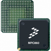
MC68360VR25VL Freescale Semiconductor, MC68360VR25VL Datasheet - Page 540

MC68360VR25VL
Manufacturer Part Number
MC68360VR25VL
Description
IC MPU QUICC 25MHZ 357-PBGA
Manufacturer
Freescale Semiconductor
Datasheets
1.MC68EN360VR25L.pdf
(14 pages)
2.MC68EN360VR25L.pdf
(2 pages)
3.MC68360AI25L.pdf
(962 pages)
Specifications of MC68360VR25VL
Processor Type
M683xx 32-Bit
Speed
25MHz
Voltage
3.3V
Mounting Type
Surface Mount
Package / Case
357-PBGA
Family Name
M68000
Device Core
ColdFire
Device Core Size
32b
Frequency (max)
25MHz
Instruction Set Architecture
RISC
Operating Supply Voltage (max)
3.3V
Operating Supply Voltage (min)
2.7V
Operating Temp Range
0C to 70C
Operating Temperature Classification
Commercial
Mounting
Surface Mount
Pin Count
357
Package Type
BGA
Lead Free Status / RoHS Status
Lead free / RoHS Compliant
Features
-
Lead Free Status / Rohs Status
Compliant
Available stocks
Company
Part Number
Manufacturer
Quantity
Price
Company:
Part Number:
MC68360VR25VL
Manufacturer:
Exar
Quantity:
160
Company:
Part Number:
MC68360VR25VL
Manufacturer:
Freescale Semiconductor
Quantity:
10 000
Company:
Part Number:
MC68360VR25VLR2
Manufacturer:
Freescale Semiconductor
Quantity:
10 000
- Current page: 540 of 962
- Download datasheet (4Mb)
Serial Communication Controllers (SCCs)
Tx Data Buffer Pointer
7.10.20.14 BISYNC EVENT REGISTER (SCCE). The SCCE is called the BISYNC event
register when the SCC is operating as a BISYNC controller. It is a 16-bit register used to
report events recognized by the BISYNC channel and to generate interrupts. On recognition
of an event, the BISYNC controller will set the corresponding bit in the BISYNC event reg-
ister. Interrupts generated by this register may be masked in the BISYNC mask register.
The BISYNC event register is a memory-mapped register that may be read at any time. A
bit is reset by writing a one (writing a zero does not affect a bit’s value). More than one bit
may be reset at a time. All unmasked bits must be reset before the CP will negate the inter-
nal interrupt request signal. This register is cleared at reset.
Bits 15–13, 9, 8, 6, 5—Reserved
GLr—Glitch on Rx
GLt—Glitch on Tx
DCC—DPLL CS Changed
GRA—Graceful Stop Complete
7-216
15
The transmit buffer pointer, which always points to the first byte of the associated data
buffer, may be even or odd. The buffer may reside in either internal or external memory.
A clock glitch was detected by this SCC on the receive clock.
A clock glitch was detected by this SCC on the transmit clock.
The carrier sense status as generated by the DPLL has changed state. The real-time sta-
tus may be found in SCCS. This is not the CD pin status that is discussed elsewhere; it is
only valid when the DPLL is used.
A graceful stop, which was initiated by the GRACEFUL STOP TRANSMIT command, is
now complete. This bit is set as soon the transmitter has finished transmitting any mes-
14
—
13
GLr
12
GLt
11
Freescale Semiconductor, Inc.
For More Information On This Product,
DCC
10
MC68360 USER’S MANUAL
Go to: www.freescale.com
—
9
—
8
GRA
7
—
6
—
5
TXE
4
RCH
3
BSY
2
TX
1
RX
0
Related parts for MC68360VR25VL
Image
Part Number
Description
Manufacturer
Datasheet
Request
R
Part Number:
Description:
Manufacturer:
Freescale Semiconductor, Inc
Datasheet:

Part Number:
Description:
MC68360 MC68360 Multiple Ethernet Channels on the QUICC
Manufacturer:
Motorola / Freescale Semiconductor

Part Number:
Description:
MC68360 Implementing an 8 bit Eprom for an MC68EC040-MC68360 System
Manufacturer:
Motorola / Freescale Semiconductor

Part Number:
Description:
MC68360 Interfacing the MC68060 to the MC68360
Manufacturer:
Motorola / Freescale Semiconductor

Part Number:
Description:
MC68360 MC68360 RAM Microcode Package Option Overview
Manufacturer:
Motorola / Freescale Semiconductor

Part Number:
Description:
MC68360 MC68360 CPM-CPU Interaction
Manufacturer:
Motorola / Freescale Semiconductor

Part Number:
Description:
MC68360 Interfacing SDRAM to the MC68360 QUICC Device
Manufacturer:
Motorola / Freescale Semiconductor

Part Number:
Description:
MC68360 Interfacing the QUICC to a MCM516400 (4Mx4 10-12 column-row) DRAM
Manufacturer:
Motorola / Freescale Semiconductor

Part Number:
Description:
MC68360 Interfacing the 68360 (QUICC) to T1-E1 Systems
Manufacturer:
Motorola / Freescale Semiconductor

Part Number:
Description:
MC68360 Multiple QUICC Design Concept
Manufacturer:
Motorola / Freescale Semiconductor
Part Number:
Description:
Manufacturer:
Freescale Semiconductor, Inc
Datasheet:
Part Number:
Description:
Manufacturer:
Freescale Semiconductor, Inc
Datasheet:
Part Number:
Description:
Manufacturer:
Freescale Semiconductor, Inc
Datasheet:
Part Number:
Description:
Manufacturer:
Freescale Semiconductor, Inc
Datasheet:
Part Number:
Description:
Manufacturer:
Freescale Semiconductor, Inc
Datasheet:


