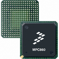
MC68360VR25VL Freescale Semiconductor, MC68360VR25VL Datasheet - Page 557

MC68360VR25VL
Manufacturer Part Number
MC68360VR25VL
Description
IC MPU QUICC 25MHZ 357-PBGA
Manufacturer
Freescale Semiconductor
Datasheets
1.MC68EN360VR25L.pdf
(14 pages)
2.MC68EN360VR25L.pdf
(2 pages)
3.MC68360AI25L.pdf
(962 pages)
Specifications of MC68360VR25VL
Processor Type
M683xx 32-Bit
Speed
25MHz
Voltage
3.3V
Mounting Type
Surface Mount
Package / Case
357-PBGA
Family Name
M68000
Device Core
ColdFire
Device Core Size
32b
Frequency (max)
25MHz
Instruction Set Architecture
RISC
Operating Supply Voltage (max)
3.3V
Operating Supply Voltage (min)
2.7V
Operating Temp Range
0C to 70C
Operating Temperature Classification
Commercial
Mounting
Surface Mount
Pin Count
357
Package Type
BGA
Lead Free Status / RoHS Status
Lead free / RoHS Compliant
Features
-
Lead Free Status / Rohs Status
Compliant
Available stocks
Company
Part Number
Manufacturer
Quantity
Price
Company:
Part Number:
MC68360VR25VL
Manufacturer:
Exar
Quantity:
160
Company:
Part Number:
MC68360VR25VL
Manufacturer:
Freescale Semiconductor
Quantity:
10 000
Company:
Part Number:
MC68360VR25VLR2
Manufacturer:
Freescale Semiconductor
Quantity:
10 000
- Current page: 557 of 962
- Download datasheet (4Mb)
TX—Tx Buffer
RX—Rx Buffer
7.10.21.12 TRANSPARENT MASK REGISTER (SCCM). The SCCM is referred to as the
transparent mask register when the SCC is operating in transparent mode. It is a 16-bit read-
write register that has the same bit format as the transparent event register. If a bit in the
transparent mask register is a one, the corresponding interrupt in the event register will be
enabled. If the bit is zero, the corresponding interrupt in the event register will be masked.
This register is cleared upon reset.
7.10.21.13 SCC STATUS REGISTER (SCCS). The SCCS is an 8-bit read-only register that
allows the user to monitor real-time status conditions on the RXD line. The real-time status
of the CTS and CD pins are part of the port C parallel I/O.
CS—Carrier Sense (DPLL)
7.10.21.14 SCC TRANSPARENT EXAMPLE. The following list is an initialization se-
quence for an SCC transparent channel. The transmitter and receiver are both enabled, but
operate independently of each other; they implement the connection shown on QUICC 2 in
Figure 7-64. Both transmit and receive clocks are provided externally to QUICC 2 using the
CLK7 pin. SCC4 is used. The transparent controller is configured with the RTS4 and CD4
pins active. CTS4 is grounded internally by the configuration in port C. A 16-bit CRC-CCITT
is sent with each transparent frame. The FIFOs are configured for fast operation.
A buffer has been transmitted. This bit is set no sooner than when the last bit of the last
byte of the buffer begins its transmission, assuming the L-bit of the Tx BD is set. If the L-
bit is not set, TX is set when the last byte of data is written to the transmit FIFO.
A complete buffer has been received on the SCC channel. This bit is set no sooner than
two serial clocks after the last bit of the last byte in which the buffer is received on the RXD
pin.
This bit shows the real-time carrier sense of the line as determined by the DPLL, if it is
used.
1. The SDCR (SDMA Configuration Register) should be initialized to $0740, rather than
2. Configure the port A pins to enable the TXD4 and RXD4 pins. Write PAPAR bits 6
3. Configure the port C pins to enable RTS4, CTS4, and CD4. Write PCPAR bit 3 with
4. Configure port A to enable the CLK7 pin. Write PAPAR bit 14 with a one. Write
0 = The DPLL does not sense a carrier.
1 = The DPLL does sense a carrier.
being left at its default value of $0000.
and 7 with ones. Write PADIR bits 6 and 7 with zeros. Write PAODR bits 6 and 7
with zeros.
one and bit 11 with zero. Write PCDIR bits 3 and 11 with zero. Write PCSO bit 11
with one and bit 10 with zero.
Freescale Semiconductor, Inc.
—
7
For More Information On This Product,
—
6
MC68360 USER’S MANUAL
Go to: www.freescale.com
—
5
—
4
—
3
Serial Communication Controllers (SCCs)
—
2
CS
1
—
0
Related parts for MC68360VR25VL
Image
Part Number
Description
Manufacturer
Datasheet
Request
R
Part Number:
Description:
Manufacturer:
Freescale Semiconductor, Inc
Datasheet:

Part Number:
Description:
MC68360 MC68360 Multiple Ethernet Channels on the QUICC
Manufacturer:
Motorola / Freescale Semiconductor

Part Number:
Description:
MC68360 Implementing an 8 bit Eprom for an MC68EC040-MC68360 System
Manufacturer:
Motorola / Freescale Semiconductor

Part Number:
Description:
MC68360 Interfacing the MC68060 to the MC68360
Manufacturer:
Motorola / Freescale Semiconductor

Part Number:
Description:
MC68360 MC68360 RAM Microcode Package Option Overview
Manufacturer:
Motorola / Freescale Semiconductor

Part Number:
Description:
MC68360 MC68360 CPM-CPU Interaction
Manufacturer:
Motorola / Freescale Semiconductor

Part Number:
Description:
MC68360 Interfacing SDRAM to the MC68360 QUICC Device
Manufacturer:
Motorola / Freescale Semiconductor

Part Number:
Description:
MC68360 Interfacing the QUICC to a MCM516400 (4Mx4 10-12 column-row) DRAM
Manufacturer:
Motorola / Freescale Semiconductor

Part Number:
Description:
MC68360 Interfacing the 68360 (QUICC) to T1-E1 Systems
Manufacturer:
Motorola / Freescale Semiconductor

Part Number:
Description:
MC68360 Multiple QUICC Design Concept
Manufacturer:
Motorola / Freescale Semiconductor
Part Number:
Description:
Manufacturer:
Freescale Semiconductor, Inc
Datasheet:
Part Number:
Description:
Manufacturer:
Freescale Semiconductor, Inc
Datasheet:
Part Number:
Description:
Manufacturer:
Freescale Semiconductor, Inc
Datasheet:
Part Number:
Description:
Manufacturer:
Freescale Semiconductor, Inc
Datasheet:
Part Number:
Description:
Manufacturer:
Freescale Semiconductor, Inc
Datasheet:


