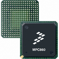
MC68360VR25VL Freescale Semiconductor, MC68360VR25VL Datasheet - Page 653

MC68360VR25VL
Manufacturer Part Number
MC68360VR25VL
Description
IC MPU QUICC 25MHZ 357-PBGA
Manufacturer
Freescale Semiconductor
Datasheets
1.MC68EN360VR25L.pdf
(14 pages)
2.MC68EN360VR25L.pdf
(2 pages)
3.MC68360AI25L.pdf
(962 pages)
Specifications of MC68360VR25VL
Processor Type
M683xx 32-Bit
Speed
25MHz
Voltage
3.3V
Mounting Type
Surface Mount
Package / Case
357-PBGA
Family Name
M68000
Device Core
ColdFire
Device Core Size
32b
Frequency (max)
25MHz
Instruction Set Architecture
RISC
Operating Supply Voltage (max)
3.3V
Operating Supply Voltage (min)
2.7V
Operating Temp Range
0C to 70C
Operating Temperature Classification
Commercial
Mounting
Surface Mount
Pin Count
357
Package Type
BGA
Lead Free Status / RoHS Status
Lead free / RoHS Compliant
Features
-
Lead Free Status / Rohs Status
Compliant
Available stocks
Company
Part Number
Manufacturer
Quantity
Price
Company:
Part Number:
MC68360VR25VL
Manufacturer:
Exar
Quantity:
160
Company:
Part Number:
MC68360VR25VL
Manufacturer:
Freescale Semiconductor
Quantity:
10 000
Company:
Part Number:
MC68360VR25VLR2
Manufacturer:
Freescale Semiconductor
Quantity:
10 000
- Current page: 653 of 962
- Download datasheet (4Mb)
RXB—Rx Buffer
7.12.5.7 SPI MASK REGISTER (SPIM). The SPIM is an 8-bit read-write register that has
the same bit formats as the SPI event register. If a bit in the SPIM is one, the corresponding
interrupt in the SPIE is enabled. If the bit is zero, the corresponding interrupt in the SPIE will
be masked. This register is cleared at reset.
7.12.6 SPI Master Example
The following list is an initialization sequence for a high-speed use of the SPI as a master.
A buffer has been received. This bit is set after the last character has been written to the
receive buffer and the Rx BD is closed.
1. The SDCR (SDMA Configuration Register) should be initialized to $0740, rather than
2. Write RBASE and TBASE in the SPI parameter RAM to point to the Rx BD and Tx
3. Configure a parallel I/O pin to operate as the SPI select pin if needed. Supposing
4. Write RBASE and TBASE in the SPI parameter RAM to point to the Rx BD and Tx
5. Program the CR to execute the INIT RX & TX PARAMS command for this channel.
6. Write RFCR with $18 and TFCR with $18 for normal operation.
7. Write MRBLR with the maximum number of bytes per receive buffer. For this case,
8. Initialize the Rx BD. Assume the Rx data buffer is at $00001000 in main memory.
9. Initialize the Tx BD. Assume the Tx data buffer is at $00002000 in main memory
10. Write $FF to the SPIE to clear any previous events.
11. Write $37 to the SPIM to enable all possible SPI interrupts.
being left at its default value of $0000.
BD in the dual-port RAM. Assuming one Rx BD at the beginning of dual-port RAM
and one Tx BD following that Rx BD, write RBASE with $0000 and TBASE with
$0008.
PB0 is chosen, write PBODR bit 0 with a zero, PBDIR bit 0 with a one, and PBPAR
bit 0 with a zero. Write PBDAT bit 0 with a zero to constantly assert the select pin.
BD in the dual-port RAM. Assuming one Rx BD at the beginning of dual-port RAM
and one Tx BD following that Rx BD, write RBASE with $0000 and TBASE with
$0008.
For instance, to execute this command for SCC1, write $0001 to the CR. This com-
mand causes the RBPTR and TBPTR parameters of the serial channel to be updated
with the new values just programmed into RBASE and TBASE.
assume 16 bytes, so MRBLR = $0010.
Write $B000 to Rx_BD_Status. Write $0000 to Rx_BD_Length (not required—
done for instructional purposes only). Write $00001000 to Rx_BD_Pointer.
and contains five 8-bit characters. Write $B800 to Tx_BD_Status. Write $0005 to
Tx_BD_Length. Write $00002000 to Tx_BD_Pointer.
In the case of multi-master operation, the SPISEL pin should
also be enabled to internally connect to the SPI.
Freescale Semiconductor, Inc.
For More Information On This Product,
MC68360 USER’S MANUAL
Go to: www.freescale.com
NOTE
Serial Peripheral Interface (SPI)
Related parts for MC68360VR25VL
Image
Part Number
Description
Manufacturer
Datasheet
Request
R
Part Number:
Description:
Manufacturer:
Freescale Semiconductor, Inc
Datasheet:

Part Number:
Description:
MC68360 MC68360 Multiple Ethernet Channels on the QUICC
Manufacturer:
Motorola / Freescale Semiconductor

Part Number:
Description:
MC68360 Implementing an 8 bit Eprom for an MC68EC040-MC68360 System
Manufacturer:
Motorola / Freescale Semiconductor

Part Number:
Description:
MC68360 Interfacing the MC68060 to the MC68360
Manufacturer:
Motorola / Freescale Semiconductor

Part Number:
Description:
MC68360 MC68360 RAM Microcode Package Option Overview
Manufacturer:
Motorola / Freescale Semiconductor

Part Number:
Description:
MC68360 MC68360 CPM-CPU Interaction
Manufacturer:
Motorola / Freescale Semiconductor

Part Number:
Description:
MC68360 Interfacing SDRAM to the MC68360 QUICC Device
Manufacturer:
Motorola / Freescale Semiconductor

Part Number:
Description:
MC68360 Interfacing the QUICC to a MCM516400 (4Mx4 10-12 column-row) DRAM
Manufacturer:
Motorola / Freescale Semiconductor

Part Number:
Description:
MC68360 Interfacing the 68360 (QUICC) to T1-E1 Systems
Manufacturer:
Motorola / Freescale Semiconductor

Part Number:
Description:
MC68360 Multiple QUICC Design Concept
Manufacturer:
Motorola / Freescale Semiconductor
Part Number:
Description:
Manufacturer:
Freescale Semiconductor, Inc
Datasheet:
Part Number:
Description:
Manufacturer:
Freescale Semiconductor, Inc
Datasheet:
Part Number:
Description:
Manufacturer:
Freescale Semiconductor, Inc
Datasheet:
Part Number:
Description:
Manufacturer:
Freescale Semiconductor, Inc
Datasheet:
Part Number:
Description:
Manufacturer:
Freescale Semiconductor, Inc
Datasheet:


