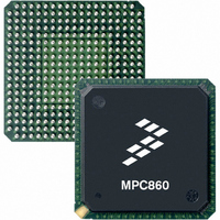
MC68360VR25VL Freescale Semiconductor, MC68360VR25VL Datasheet - Page 687

MC68360VR25VL
Manufacturer Part Number
MC68360VR25VL
Description
IC MPU QUICC 25MHZ 357-PBGA
Manufacturer
Freescale Semiconductor
Datasheets
1.MC68EN360VR25L.pdf
(14 pages)
2.MC68EN360VR25L.pdf
(2 pages)
3.MC68360AI25L.pdf
(962 pages)
Specifications of MC68360VR25VL
Processor Type
M683xx 32-Bit
Speed
25MHz
Voltage
3.3V
Mounting Type
Surface Mount
Package / Case
357-PBGA
Family Name
M68000
Device Core
ColdFire
Device Core Size
32b
Frequency (max)
25MHz
Instruction Set Architecture
RISC
Operating Supply Voltage (max)
3.3V
Operating Supply Voltage (min)
2.7V
Operating Temp Range
0C to 70C
Operating Temperature Classification
Commercial
Mounting
Surface Mount
Pin Count
357
Package Type
BGA
Lead Free Status / RoHS Status
Lead free / RoHS Compliant
Features
-
Lead Free Status / Rohs Status
Compliant
Available stocks
Company
Part Number
Manufacturer
Quantity
Price
Company:
Part Number:
MC68360VR25VL
Manufacturer:
Exar
Quantity:
160
Company:
Part Number:
MC68360VR25VL
Manufacturer:
Freescale Semiconductor
Quantity:
10 000
Company:
Part Number:
MC68360VR25VLR2
Manufacturer:
Freescale Semiconductor
Quantity:
10 000
- Current page: 687 of 962
- Download datasheet (4Mb)
7.14.7 Port B Registers
Port B has four memory-mapped, read-write, 16-bit control registers.
7.14.7.1 PORT B OPEN-DRAIN REGISTER (PBODR). The PBODR is a 16-bit register
that indicates a normal or wired-OR configuration of the port pins. (Bits 17 and 16 of PBODR
do not exist.) PBODR is cleared at system reset.
OD15
15
Signal
PB10
PB11
PB12
PB13
PB14
PB15
PB16
PB17
PB0
PB1
PB2
PB3
PB4
PB5
PB6
PB7
PB8
PB9
OD14
14
OD13
The user may freely configure any of the previous functions to
be output onto two pins at once, although there is typically no ad-
vantage in doing this (except in the case of a large fanout, where
it is advantageous to share the load between two pins).
13
PBPAR = 0
PORT B10
PORT B11
PORT B12
PORT B13
PORT B14
PORT B15
PORT B16
PORT B17
PORT B0
PORT B1
PORT B2
PORT B3
PORT B4
PORT B5
PORT B6
PORT B7
PORT B8
PORT B9
OD12
12
Freescale Semiconductor, Inc.
OD11
11
For More Information On This Product,
Table 7-20. Port B Pin Assignment
OD10
PBDIR = 0
SYMSYN1
SYMSYN2
10
SMRXD1
SMRXD2
SMTXD1
SMTXD2
RRJCT1
RRJCT2
BRGO4
BRGO1
BRGO2
RSTR2
L1ST1
L1ST2
L1ST3
L1ST4
MC68360 USER’S MANUAL
Go to: www.freescale.com
—
—
OD9
9
PBPAR = 1
OD8
NOTE
8
Pin Function
t
OD7
7
RTS3/L1RQB
RTS4/L1RQA
PBDIR = 1
L1CLKOB
L1CLKOA
SPIMOSI
SPIMISO
RSTRT1
SPISEL
SPICLK
BRGO3
DREQ1
DONE1
DONE2
DREQ2
DACK1
DACK2
RTS1
RTS2
OD6
6
OD5
5
OD4
4
SPIMISO = SPIMOSI
SYMSYN2 = GND
Input to On-Chip
OD3
SMRXD2 = GND
SPICLK = GND
DONE1 = V
DREQ1 = GND
3
Peripherals
V
V
V
GND
OD2
Parallel I/O Ports
DD
DD
—
DD
—
—
—
—
—
—
—
2
DD
OD1
1
OD0
0
Related parts for MC68360VR25VL
Image
Part Number
Description
Manufacturer
Datasheet
Request
R
Part Number:
Description:
Manufacturer:
Freescale Semiconductor, Inc
Datasheet:

Part Number:
Description:
MC68360 MC68360 Multiple Ethernet Channels on the QUICC
Manufacturer:
Motorola / Freescale Semiconductor

Part Number:
Description:
MC68360 Implementing an 8 bit Eprom for an MC68EC040-MC68360 System
Manufacturer:
Motorola / Freescale Semiconductor

Part Number:
Description:
MC68360 Interfacing the MC68060 to the MC68360
Manufacturer:
Motorola / Freescale Semiconductor

Part Number:
Description:
MC68360 MC68360 RAM Microcode Package Option Overview
Manufacturer:
Motorola / Freescale Semiconductor

Part Number:
Description:
MC68360 MC68360 CPM-CPU Interaction
Manufacturer:
Motorola / Freescale Semiconductor

Part Number:
Description:
MC68360 Interfacing SDRAM to the MC68360 QUICC Device
Manufacturer:
Motorola / Freescale Semiconductor

Part Number:
Description:
MC68360 Interfacing the QUICC to a MCM516400 (4Mx4 10-12 column-row) DRAM
Manufacturer:
Motorola / Freescale Semiconductor

Part Number:
Description:
MC68360 Interfacing the 68360 (QUICC) to T1-E1 Systems
Manufacturer:
Motorola / Freescale Semiconductor

Part Number:
Description:
MC68360 Multiple QUICC Design Concept
Manufacturer:
Motorola / Freescale Semiconductor
Part Number:
Description:
Manufacturer:
Freescale Semiconductor, Inc
Datasheet:
Part Number:
Description:
Manufacturer:
Freescale Semiconductor, Inc
Datasheet:
Part Number:
Description:
Manufacturer:
Freescale Semiconductor, Inc
Datasheet:
Part Number:
Description:
Manufacturer:
Freescale Semiconductor, Inc
Datasheet:
Part Number:
Description:
Manufacturer:
Freescale Semiconductor, Inc
Datasheet:


