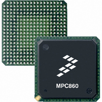
MC68360VR25VL Freescale Semiconductor, MC68360VR25VL Datasheet - Page 241

MC68360VR25VL
Manufacturer Part Number
MC68360VR25VL
Description
IC MPU QUICC 25MHZ 357-PBGA
Manufacturer
Freescale Semiconductor
Datasheets
1.MC68EN360VR25L.pdf
(14 pages)
2.MC68EN360VR25L.pdf
(2 pages)
3.MC68360AI25L.pdf
(962 pages)
Specifications of MC68360VR25VL
Processor Type
M683xx 32-Bit
Speed
25MHz
Voltage
3.3V
Mounting Type
Surface Mount
Package / Case
357-PBGA
Family Name
M68000
Device Core
ColdFire
Device Core Size
32b
Frequency (max)
25MHz
Instruction Set Architecture
RISC
Operating Supply Voltage (max)
3.3V
Operating Supply Voltage (min)
2.7V
Operating Temp Range
0C to 70C
Operating Temperature Classification
Commercial
Mounting
Surface Mount
Pin Count
357
Package Type
BGA
Lead Free Status / RoHS Status
Lead free / RoHS Compliant
Features
-
Lead Free Status / Rohs Status
Compliant
Available stocks
Company
Part Number
Manufacturer
Quantity
Price
Company:
Part Number:
MC68360VR25VL
Manufacturer:
Exar
Quantity:
160
Company:
Part Number:
MC68360VR25VL
Manufacturer:
Freescale Semiconductor
Quantity:
10 000
Company:
Part Number:
MC68360VR25VLR2
Manufacturer:
Freescale Semiconductor
Quantity:
10 000
- Current page: 241 of 962
- Download datasheet (4Mb)
5.7.2.12 CONTROL INSTRUCTIONS. The control instruction table indicates the number of
clock periods needed for the processor to perform the specified operation on the given
addressing mode. Footnotes indicate when to account for the appropriate EA times. The
total number of clock cycles is outside the parentheses. The numbers inside parentheses (r/
p/w) are included in the total clock cycle number. All timing data assumes two-clock reads
and writes.
ANDI
EORI
ORI
ANDI
EORI
ORI
BSR.B
BSR.W
BSR.L
CHK
CHK
CHK2 (Save) FEA , Dn (no ex)
CHK2 (Op) FEA , Dn (no ex)
CHK2 (Save) FEA , Dn (ex)
CHK2 (Op) FEA , Dn (ex)
JMP
JSR
LEA
LINK.W An, #
LINK.L An, #
NOP
PEA
RTD
RTR
RTS
UNLK
X
NOTE: The CHK2 instruction involves a save step that other instructions do not have. To cal-
culate the total instruction time, calculate the save, the EA, and the operation execution times;
then combine in the order listed using the equations given in 5.7.1 Resource Scheduling.
=
#, SR
#, SR
#, SR
#, CCR
#, CCR
#, CCR
#
An
FEA , Dn (no ex)
FEA , Dn (ex)
CEA
CEA
CEA , An
CEA
There is one bus cycle for byte and word operands and two bus cycles for long-word
operands. For long-word bus cycles, add two clocks to the tail and to the number of
cycles.
Timing is calculated with the CPU32+ in 16-bit mode.
Instruction
Freescale Semiconductor, Inc.
For More Information On This Product,
MC68360 USER’S MANUAL
Go to: www.freescale.com
Head
0
0
0
2
2
2
3
3
1
2
2
1
2
1
2
0
3
0
2
0
0
0
1
1
1
1
Tail
0
0
0
0
1
0
1
0
0
0
0
0
0
2
2
2
2
2
2
2
2
2
2
2
2
2
52(X
18(X/0/0)
12(0/2/0)
12(0/2/0)
12(0/2/0)
13(0/2/2)
13(0/2/2)
13(0/2/2)
42(2/2/6)
13(0/2/2)
10(0/2/2)
10(0/3/2)
12(2/2/0)
14(3/2/0)
12(2/2/0)
6(0/2/0)
6(0/2/0)
6(0/2/0)
8(0/1/0)
3(0/1/0)
3(0/1/0)
6(0/2/0)
2(0/1/0)
2(0/1/0)
8(0/1/2)
9(2/1/0)
Cycles
2/1/6)
CPU32+
Related parts for MC68360VR25VL
Image
Part Number
Description
Manufacturer
Datasheet
Request
R
Part Number:
Description:
Manufacturer:
Freescale Semiconductor, Inc
Datasheet:

Part Number:
Description:
MC68360 MC68360 Multiple Ethernet Channels on the QUICC
Manufacturer:
Motorola / Freescale Semiconductor

Part Number:
Description:
MC68360 Implementing an 8 bit Eprom for an MC68EC040-MC68360 System
Manufacturer:
Motorola / Freescale Semiconductor

Part Number:
Description:
MC68360 Interfacing the MC68060 to the MC68360
Manufacturer:
Motorola / Freescale Semiconductor

Part Number:
Description:
MC68360 MC68360 RAM Microcode Package Option Overview
Manufacturer:
Motorola / Freescale Semiconductor

Part Number:
Description:
MC68360 MC68360 CPM-CPU Interaction
Manufacturer:
Motorola / Freescale Semiconductor

Part Number:
Description:
MC68360 Interfacing SDRAM to the MC68360 QUICC Device
Manufacturer:
Motorola / Freescale Semiconductor

Part Number:
Description:
MC68360 Interfacing the QUICC to a MCM516400 (4Mx4 10-12 column-row) DRAM
Manufacturer:
Motorola / Freescale Semiconductor

Part Number:
Description:
MC68360 Interfacing the 68360 (QUICC) to T1-E1 Systems
Manufacturer:
Motorola / Freescale Semiconductor

Part Number:
Description:
MC68360 Multiple QUICC Design Concept
Manufacturer:
Motorola / Freescale Semiconductor
Part Number:
Description:
Manufacturer:
Freescale Semiconductor, Inc
Datasheet:
Part Number:
Description:
Manufacturer:
Freescale Semiconductor, Inc
Datasheet:
Part Number:
Description:
Manufacturer:
Freescale Semiconductor, Inc
Datasheet:
Part Number:
Description:
Manufacturer:
Freescale Semiconductor, Inc
Datasheet:
Part Number:
Description:
Manufacturer:
Freescale Semiconductor, Inc
Datasheet:


