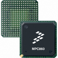
MC68360VR25VL Freescale Semiconductor, MC68360VR25VL Datasheet - Page 487

MC68360VR25VL
Manufacturer Part Number
MC68360VR25VL
Description
IC MPU QUICC 25MHZ 357-PBGA
Manufacturer
Freescale Semiconductor
Datasheets
1.MC68EN360VR25L.pdf
(14 pages)
2.MC68EN360VR25L.pdf
(2 pages)
3.MC68360AI25L.pdf
(962 pages)
Specifications of MC68360VR25VL
Processor Type
M683xx 32-Bit
Speed
25MHz
Voltage
3.3V
Mounting Type
Surface Mount
Package / Case
357-PBGA
Family Name
M68000
Device Core
ColdFire
Device Core Size
32b
Frequency (max)
25MHz
Instruction Set Architecture
RISC
Operating Supply Voltage (max)
3.3V
Operating Supply Voltage (min)
2.7V
Operating Temp Range
0C to 70C
Operating Temperature Classification
Commercial
Mounting
Surface Mount
Pin Count
357
Package Type
BGA
Lead Free Status / RoHS Status
Lead free / RoHS Compliant
Features
-
Lead Free Status / Rohs Status
Compliant
Available stocks
Company
Part Number
Manufacturer
Quantity
Price
Company:
Part Number:
MC68360VR25VL
Manufacturer:
Exar
Quantity:
160
Company:
Part Number:
MC68360VR25VL
Manufacturer:
Freescale Semiconductor
Quantity:
10 000
Company:
Part Number:
MC68360VR25VLR2
Manufacturer:
Freescale Semiconductor
Quantity:
10 000
- Current page: 487 of 962
- Download datasheet (4Mb)
Rx Data Buffer Pointer
7.10.16.17 UART TRANSMIT BUFFER DESCRIPTOR (TX BD). Data is presented to the
CP for transmission on an SCC channel by arranging it in buffers referenced by the chan-
nel’s Tx BD table. The CP confirms transmission or indicates error conditions via the BDs to
inform the processor that the buffers have been serviced.
R—Ready
W—Wrap (Final BD in Table)
I—Interrupt
CR—Clear-to-Send Report
The receive buffer pointer, which always points to the first location of the associated data
buffer, may be even or odd. The buffer may reside in either internal or external memory.
This bit allows a choice of either no delay between buffers transmitted in UART mode, or
a more accurate CTS lost error reporting and three bits of idle between buffers.
OFFSET + 0
OFFSET + 2
OFFSET + 4
OFFSET + 6
NOTE: Entries in boldface must be initialized by the user.
0 = The data buffer associated with this BD is not ready for transmission. The user is
1 = The data buffer, which has been prepared for transmission by the user, has not
0 = This is not the last BD in the Tx BD table.
1 = This is the last BD in the TxBD in the table. After this buffer has been used, the CP
0 = No interrupt is generated after this buffer has been serviced.
1 = The TX bit in the UART event register will be set when this buffer has been serviced
0 = The buffer following this buffer will be transmitted with no delay (assuming it is
1 = Normal CTS lost (CT bit) error reporting, and three bits of idle occur between back-
free to manipulate this BD or its associated data buffer. The CP clears this bit after
the buffer has been transmitted or after an error condition is encountered.
been transmitted or is currently being transmitted. No fields of this BD may be writ-
ten by the user once this bit is set.
will transmit data from the first BD in the table (the BD pointed to by TBASE). The
number of Tx BDs in this table is programmable, and is determined only by the W-
bit and the overall space constraints of the dual-port RAM.
by the CP, which can cause an interrupt.
ready), but the CT bit may not be set in the correct Tx BD or may not be set at all
in a CTS lost condition. Asynchronous flow control, however, continues to function
normally.
to-back buffers.
15
R
14
—
13
W
Freescale Semiconductor, Inc.
For More Information On This Product,
12
I
CR
11
MC68360 USER’S MANUAL
Go to: www.freescale.com
10
A
CM
TX DATA BUFFER POINTER
9
DATA LENGTH
8
P
NS
7
Serial Communication Controllers (SCCs)
—
6
—
5
—
4
—
3
—
2
—
1
CT
0
Related parts for MC68360VR25VL
Image
Part Number
Description
Manufacturer
Datasheet
Request
R
Part Number:
Description:
Manufacturer:
Freescale Semiconductor, Inc
Datasheet:

Part Number:
Description:
MC68360 MC68360 Multiple Ethernet Channels on the QUICC
Manufacturer:
Motorola / Freescale Semiconductor

Part Number:
Description:
MC68360 Implementing an 8 bit Eprom for an MC68EC040-MC68360 System
Manufacturer:
Motorola / Freescale Semiconductor

Part Number:
Description:
MC68360 Interfacing the MC68060 to the MC68360
Manufacturer:
Motorola / Freescale Semiconductor

Part Number:
Description:
MC68360 MC68360 RAM Microcode Package Option Overview
Manufacturer:
Motorola / Freescale Semiconductor

Part Number:
Description:
MC68360 MC68360 CPM-CPU Interaction
Manufacturer:
Motorola / Freescale Semiconductor

Part Number:
Description:
MC68360 Interfacing SDRAM to the MC68360 QUICC Device
Manufacturer:
Motorola / Freescale Semiconductor

Part Number:
Description:
MC68360 Interfacing the QUICC to a MCM516400 (4Mx4 10-12 column-row) DRAM
Manufacturer:
Motorola / Freescale Semiconductor

Part Number:
Description:
MC68360 Interfacing the 68360 (QUICC) to T1-E1 Systems
Manufacturer:
Motorola / Freescale Semiconductor

Part Number:
Description:
MC68360 Multiple QUICC Design Concept
Manufacturer:
Motorola / Freescale Semiconductor
Part Number:
Description:
Manufacturer:
Freescale Semiconductor, Inc
Datasheet:
Part Number:
Description:
Manufacturer:
Freescale Semiconductor, Inc
Datasheet:
Part Number:
Description:
Manufacturer:
Freescale Semiconductor, Inc
Datasheet:
Part Number:
Description:
Manufacturer:
Freescale Semiconductor, Inc
Datasheet:
Part Number:
Description:
Manufacturer:
Freescale Semiconductor, Inc
Datasheet:


