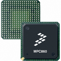
MC68360VR25VL Freescale Semiconductor, MC68360VR25VL Datasheet - Page 358

MC68360VR25VL
Manufacturer Part Number
MC68360VR25VL
Description
IC MPU QUICC 25MHZ 357-PBGA
Manufacturer
Freescale Semiconductor
Datasheets
1.MC68EN360VR25L.pdf
(14 pages)
2.MC68EN360VR25L.pdf
(2 pages)
3.MC68360AI25L.pdf
(962 pages)
Specifications of MC68360VR25VL
Processor Type
M683xx 32-Bit
Speed
25MHz
Voltage
3.3V
Mounting Type
Surface Mount
Package / Case
357-PBGA
Family Name
M68000
Device Core
ColdFire
Device Core Size
32b
Frequency (max)
25MHz
Instruction Set Architecture
RISC
Operating Supply Voltage (max)
3.3V
Operating Supply Voltage (min)
2.7V
Operating Temp Range
0C to 70C
Operating Temperature Classification
Commercial
Mounting
Surface Mount
Pin Count
357
Package Type
BGA
Lead Free Status / RoHS Status
Lead free / RoHS Compliant
Features
-
Lead Free Status / Rohs Status
Compliant
Available stocks
Company
Part Number
Manufacturer
Quantity
Price
Company:
Part Number:
MC68360VR25VL
Manufacturer:
Exar
Quantity:
160
Company:
Part Number:
MC68360VR25VL
Manufacturer:
Freescale Semiconductor
Quantity:
10 000
Company:
Part Number:
MC68360VR25VLR2
Manufacturer:
Freescale Semiconductor
Quantity:
10 000
- Current page: 358 of 962
- Download datasheet (4Mb)
Freescale Semiconductor, Inc.
IDMA Channels
7.6.4 IDMA Operation
Every IDMA operation involves the following steps: IDMA channel initialization, data trans-
fer, and block termination. In the initialization phase, the core (or external processor) loads
the registers with control information, initializes the IDMA BDs (if auto buffer or buffer chain-
ing is used), and then starts the channel. In the transfer phase, the IDMA accepts requests
for operand transfers and provides addressing and bus control for the transfers. The termi-
nation phase occurs when the operation is complete and the IDMA interrupts the core if
interrupts are enabled.
To initialize a block transfer operation, the user must initialize the IDMA registers. For the
auto buffer and buffer chaining modes, the IDMA BDs must be initialized with information
describing the data block, device type, request generation method, and other special control
options. See 7.6.2 IDMA Registers and 7.6.4.2.3 IDMA Commands (INIT_IDMA) for further
details.
7.6.4.1 SINGLE BUFFER. The single buffer mode is used to transfer only one buffer of
data. When the buffer has been completely transferred (transfer count exhausted or DONEx
is asserted), the IDMA channel operation is terminated, STR is cleared, and a maskable
interrupt is generated by the DONE bit in the CSR.
7.6.4.2 AUTO BUFFER AND BUFFER CHAINING. The auto buffer and the buffer chaining
modes are supported with the RISC controller by setting the RCI bit in the CMR. The host
processor should initialize the IDMA BD ring (see Figure 7-9) with the appropriate buffer
handling mode, source address, destination address, and block length. The user then sets
the STR bit in the CMR. All transfer modes described in 7.6.4.4.4 External Cycle Steal are
still valid. The function codes for the source and destination addresses are programmed as
described in 7.5.2.5 Timer Capture Registers (TCR1, TCR2, TCR3, TCR4).
7-34
MC68360 USER’S MANUAL
For More Information On This Product,
Go to: www.freescale.com
Related parts for MC68360VR25VL
Image
Part Number
Description
Manufacturer
Datasheet
Request
R
Part Number:
Description:
Manufacturer:
Freescale Semiconductor, Inc
Datasheet:

Part Number:
Description:
MC68360 MC68360 Multiple Ethernet Channels on the QUICC
Manufacturer:
Motorola / Freescale Semiconductor

Part Number:
Description:
MC68360 Implementing an 8 bit Eprom for an MC68EC040-MC68360 System
Manufacturer:
Motorola / Freescale Semiconductor

Part Number:
Description:
MC68360 Interfacing the MC68060 to the MC68360
Manufacturer:
Motorola / Freescale Semiconductor

Part Number:
Description:
MC68360 MC68360 RAM Microcode Package Option Overview
Manufacturer:
Motorola / Freescale Semiconductor

Part Number:
Description:
MC68360 MC68360 CPM-CPU Interaction
Manufacturer:
Motorola / Freescale Semiconductor

Part Number:
Description:
MC68360 Interfacing SDRAM to the MC68360 QUICC Device
Manufacturer:
Motorola / Freescale Semiconductor

Part Number:
Description:
MC68360 Interfacing the QUICC to a MCM516400 (4Mx4 10-12 column-row) DRAM
Manufacturer:
Motorola / Freescale Semiconductor

Part Number:
Description:
MC68360 Interfacing the 68360 (QUICC) to T1-E1 Systems
Manufacturer:
Motorola / Freescale Semiconductor

Part Number:
Description:
MC68360 Multiple QUICC Design Concept
Manufacturer:
Motorola / Freescale Semiconductor
Part Number:
Description:
Manufacturer:
Freescale Semiconductor, Inc
Datasheet:
Part Number:
Description:
Manufacturer:
Freescale Semiconductor, Inc
Datasheet:
Part Number:
Description:
Manufacturer:
Freescale Semiconductor, Inc
Datasheet:
Part Number:
Description:
Manufacturer:
Freescale Semiconductor, Inc
Datasheet:
Part Number:
Description:
Manufacturer:
Freescale Semiconductor, Inc
Datasheet:


