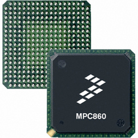
MC68360VR25VL Freescale Semiconductor, MC68360VR25VL Datasheet - Page 675

MC68360VR25VL
Manufacturer Part Number
MC68360VR25VL
Description
IC MPU QUICC 25MHZ 357-PBGA
Manufacturer
Freescale Semiconductor
Datasheets
1.MC68EN360VR25L.pdf
(14 pages)
2.MC68EN360VR25L.pdf
(2 pages)
3.MC68360AI25L.pdf
(962 pages)
Specifications of MC68360VR25VL
Processor Type
M683xx 32-Bit
Speed
25MHz
Voltage
3.3V
Mounting Type
Surface Mount
Package / Case
357-PBGA
Family Name
M68000
Device Core
ColdFire
Device Core Size
32b
Frequency (max)
25MHz
Instruction Set Architecture
RISC
Operating Supply Voltage (max)
3.3V
Operating Supply Voltage (min)
2.7V
Operating Temp Range
0C to 70C
Operating Temperature Classification
Commercial
Mounting
Surface Mount
Pin Count
357
Package Type
BGA
Lead Free Status / RoHS Status
Lead free / RoHS Compliant
Features
-
Lead Free Status / Rohs Status
Compliant
Available stocks
Company
Part Number
Manufacturer
Quantity
Price
Company:
Part Number:
MC68360VR25VL
Manufacturer:
Exar
Quantity:
160
Company:
Part Number:
MC68360VR25VL
Manufacturer:
Freescale Semiconductor
Quantity:
10 000
Company:
Part Number:
MC68360VR25VLR2
Manufacturer:
Freescale Semiconductor
Quantity:
10 000
- Current page: 675 of 962
- Download datasheet (4Mb)
Certain parameter RAM values above (marked in bold face) need to be initialized by the
user before the PIP is enabled; the others are initialized/written by the CP. Once initialized,
most parameter RAM values will not need to be accessed in user software since most of the
activity is centered around the transmit buffer descriptors, not the parameter RAM.
7.13.8.14 BUFFER DESCRIPTOR TABLE POINTER (RBASE). The RBASE entry defines
the starting location in the dual-port RAM for the PIP receiver’s set of buffer descriptors. This
provides a great deal of flexibility in how BDs are partitioned. By programming the RBASE
entry and by setting the "wrap" bit in the last BD, the user may select how many BDs to allo-
cate for the receive function. The user must initialize RBASE before enabling the channel.
7.13.8.15 CENTRONICS FUNCTION CODE REGISTER (CFCR). The FC entry contains
the value that the user would like to appear on the function code pins (FC3-0) when the
associated SDMA channel accesses memory. It also controls the byte ordering convention
to be used in the transfers.
PIP Base+12
PIP Base+14
PIP Base+18
PIP Base+1C
PIP Base+20
PIP Base+22
PIP Base+24
PIP Base+28
PIP Base+2a
PIP Base+2c
PIP Base+2E
PIP Base+30
PIP Base+32
PIP Base+34
PIP Base+36
PIP Base+38
PIP Base+3A
PIP Base+3C
PIP Base+3E
Address
.RBASE should contain a value that is divisible by 8.
Table 7-18. Centronics Receiver Parameter RAM
R_CNT
RTEMP
Res
Res
Res
Res
Res
MAX_SL
SL_CNT
CHARCTER1
CHARCTER2
CHARCTER3
CHARCTER4
CHARCTER5
CHARCTER6
CHARCTER7
CHARCTER8
RCCM
RCCR
Freescale Semiconductor, Inc.
For More Information On This Product,
Name
MC68360 USER’S MANUAL
Go to: www.freescale.com
Word
Long
Word
Word
Word
Word
Long
Word
Word
Word
Word
Word
Word
Word
Word
Word
Word
Word
Word
Width
NOTE
Rx Internal Byte Count
Rx Temp
Reserved
Reserved
Reserved
Reserved
Reserved
Maximum Silence period
Silence counter
CONTROL character 1
CONTROL character 2
CONTROL character 3
CONTROL character 4
CONTROL character 5
CONTROL character 6
CONTROL character 7
CONTROL character 8
Receive Control Character Mask
Receive Character Control Register
Description
Parallel Interface Port (PIP)
Related parts for MC68360VR25VL
Image
Part Number
Description
Manufacturer
Datasheet
Request
R
Part Number:
Description:
Manufacturer:
Freescale Semiconductor, Inc
Datasheet:

Part Number:
Description:
MC68360 MC68360 Multiple Ethernet Channels on the QUICC
Manufacturer:
Motorola / Freescale Semiconductor

Part Number:
Description:
MC68360 Implementing an 8 bit Eprom for an MC68EC040-MC68360 System
Manufacturer:
Motorola / Freescale Semiconductor

Part Number:
Description:
MC68360 Interfacing the MC68060 to the MC68360
Manufacturer:
Motorola / Freescale Semiconductor

Part Number:
Description:
MC68360 MC68360 RAM Microcode Package Option Overview
Manufacturer:
Motorola / Freescale Semiconductor

Part Number:
Description:
MC68360 MC68360 CPM-CPU Interaction
Manufacturer:
Motorola / Freescale Semiconductor

Part Number:
Description:
MC68360 Interfacing SDRAM to the MC68360 QUICC Device
Manufacturer:
Motorola / Freescale Semiconductor

Part Number:
Description:
MC68360 Interfacing the QUICC to a MCM516400 (4Mx4 10-12 column-row) DRAM
Manufacturer:
Motorola / Freescale Semiconductor

Part Number:
Description:
MC68360 Interfacing the 68360 (QUICC) to T1-E1 Systems
Manufacturer:
Motorola / Freescale Semiconductor

Part Number:
Description:
MC68360 Multiple QUICC Design Concept
Manufacturer:
Motorola / Freescale Semiconductor
Part Number:
Description:
Manufacturer:
Freescale Semiconductor, Inc
Datasheet:
Part Number:
Description:
Manufacturer:
Freescale Semiconductor, Inc
Datasheet:
Part Number:
Description:
Manufacturer:
Freescale Semiconductor, Inc
Datasheet:
Part Number:
Description:
Manufacturer:
Freescale Semiconductor, Inc
Datasheet:
Part Number:
Description:
Manufacturer:
Freescale Semiconductor, Inc
Datasheet:


