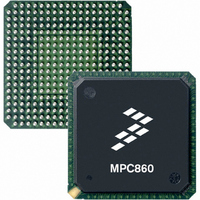
MC68360VR25VL Freescale Semiconductor, MC68360VR25VL Datasheet - Page 308

MC68360VR25VL
Manufacturer Part Number
MC68360VR25VL
Description
IC MPU QUICC 25MHZ 357-PBGA
Manufacturer
Freescale Semiconductor
Datasheets
1.MC68EN360VR25L.pdf
(14 pages)
2.MC68EN360VR25L.pdf
(2 pages)
3.MC68360AI25L.pdf
(962 pages)
Specifications of MC68360VR25VL
Processor Type
M683xx 32-Bit
Speed
25MHz
Voltage
3.3V
Mounting Type
Surface Mount
Package / Case
357-PBGA
Family Name
M68000
Device Core
ColdFire
Device Core Size
32b
Frequency (max)
25MHz
Instruction Set Architecture
RISC
Operating Supply Voltage (max)
3.3V
Operating Supply Voltage (min)
2.7V
Operating Temp Range
0C to 70C
Operating Temperature Classification
Commercial
Mounting
Surface Mount
Pin Count
357
Package Type
BGA
Lead Free Status / RoHS Status
Lead free / RoHS Compliant
Features
-
Lead Free Status / Rohs Status
Compliant
Available stocks
Company
Part Number
Manufacturer
Quantity
Price
Company:
Part Number:
MC68360VR25VL
Manufacturer:
Exar
Quantity:
160
Company:
Part Number:
MC68360VR25VL
Manufacturer:
Freescale Semiconductor
Quantity:
10 000
Company:
Part Number:
MC68360VR25VLR2
Manufacturer:
Freescale Semiconductor
Quantity:
10 000
- Current page: 308 of 962
- Download datasheet (4Mb)
System Integration Module (SIM60)
6.13 PROGRAMMING MODEL
The user interfaces with the memory controller using eight identical sets of two registers, the
BR and OR. There are also two global registers in the memory controller: the GMR and the
MSTAT.
6.13.1 Global Memory Register (GMR)
The 32-bit read-write GMR contains selections that are common to the entire memory con-
troller: DRAM refresh properties, DRAM bank properties, SRAM bank properties, and some
global SRAM/DRAM properties. The reserved bits (4–0) should be written with zero.
The following bits are used for DRAM refresh properties.
RCNT7–RCNT0—Refresh Counter Period
RFEN—Refresh Enable
RCYC1–RCYC0—Refresh Cycle Length
6-64
RCNT7 RCNT6 RCNT5 RCNT4 RCNT3 RCNT2 RCNT1 RCNT0
WBT40
31
15
These bits determine the refresh period according to the following equation:
Example: For a 25-MHz system clock and a required refresh rate of 15.6 s per row, the
RFCNT value should be 24 (decimal). 24/(25 MHz/16) = 15.36 s, which is less than the
required refresh period of 15.6 s.
These bits determine the length of a refresh cycle.
0
0
0 = DRAM refresh is disabled.
1 = DRAM refresh is enabled.
00 = The refresh cycle is 4 clocks long, and RAS is negated for 3 phases prior to being
01 = The refresh cycle is 6 clocks long, and RAS is negated for 5 phases prior to being
10 = The refresh cycle is 7 clocks long, and RAS is negated for 5 phases prior to being
11 = The refresh cycle is 8 clocks long, and RAS is negated for 5 phases prior to being
WBTQ
30
14
0
0
asserted.
asserted.
asserted.
asserted.
SYNC
29
13
0
0
EMWS
28
12
0
1
OPAR
27
11
Freescale Semiconductor, Inc.
0
0
Refresh period
For More Information On This Product,
PBEE
26
10
0
0
MC68360 USER’S MANUAL
Go to: www.freescale.com
TSS40
25
0
1
9
NCS
24
0
8
0
=
RFEN
DWQ
23
0
7
0
System clk/16
RFCNT+1
RCYC1 RCYC0
DW40
22
0
6
0
GAMX
21
0
5
0
PGS2
20
—
0
4
0
PGS1
19
—
0
3
0
SUPERVISOR SPACE ONLY
PGS0
18
—
0
2
0
DPS1
17
—
0
1
0
DPS0
16
—
0
0
0
Related parts for MC68360VR25VL
Image
Part Number
Description
Manufacturer
Datasheet
Request
R
Part Number:
Description:
Manufacturer:
Freescale Semiconductor, Inc
Datasheet:

Part Number:
Description:
MC68360 MC68360 Multiple Ethernet Channels on the QUICC
Manufacturer:
Motorola / Freescale Semiconductor

Part Number:
Description:
MC68360 Implementing an 8 bit Eprom for an MC68EC040-MC68360 System
Manufacturer:
Motorola / Freescale Semiconductor

Part Number:
Description:
MC68360 Interfacing the MC68060 to the MC68360
Manufacturer:
Motorola / Freescale Semiconductor

Part Number:
Description:
MC68360 MC68360 RAM Microcode Package Option Overview
Manufacturer:
Motorola / Freescale Semiconductor

Part Number:
Description:
MC68360 MC68360 CPM-CPU Interaction
Manufacturer:
Motorola / Freescale Semiconductor

Part Number:
Description:
MC68360 Interfacing SDRAM to the MC68360 QUICC Device
Manufacturer:
Motorola / Freescale Semiconductor

Part Number:
Description:
MC68360 Interfacing the QUICC to a MCM516400 (4Mx4 10-12 column-row) DRAM
Manufacturer:
Motorola / Freescale Semiconductor

Part Number:
Description:
MC68360 Interfacing the 68360 (QUICC) to T1-E1 Systems
Manufacturer:
Motorola / Freescale Semiconductor

Part Number:
Description:
MC68360 Multiple QUICC Design Concept
Manufacturer:
Motorola / Freescale Semiconductor
Part Number:
Description:
Manufacturer:
Freescale Semiconductor, Inc
Datasheet:
Part Number:
Description:
Manufacturer:
Freescale Semiconductor, Inc
Datasheet:
Part Number:
Description:
Manufacturer:
Freescale Semiconductor, Inc
Datasheet:
Part Number:
Description:
Manufacturer:
Freescale Semiconductor, Inc
Datasheet:
Part Number:
Description:
Manufacturer:
Freescale Semiconductor, Inc
Datasheet:


