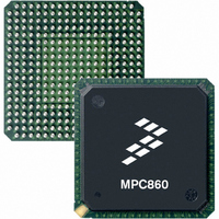
MC68360VR25VL Freescale Semiconductor, MC68360VR25VL Datasheet - Page 202

MC68360VR25VL
Manufacturer Part Number
MC68360VR25VL
Description
IC MPU QUICC 25MHZ 357-PBGA
Manufacturer
Freescale Semiconductor
Datasheets
1.MC68EN360VR25L.pdf
(14 pages)
2.MC68EN360VR25L.pdf
(2 pages)
3.MC68360AI25L.pdf
(962 pages)
Specifications of MC68360VR25VL
Processor Type
M683xx 32-Bit
Speed
25MHz
Voltage
3.3V
Mounting Type
Surface Mount
Package / Case
357-PBGA
Family Name
M68000
Device Core
ColdFire
Device Core Size
32b
Frequency (max)
25MHz
Instruction Set Architecture
RISC
Operating Supply Voltage (max)
3.3V
Operating Supply Voltage (min)
2.7V
Operating Temp Range
0C to 70C
Operating Temperature Classification
Commercial
Mounting
Surface Mount
Pin Count
357
Package Type
BGA
Lead Free Status / RoHS Status
Lead free / RoHS Compliant
Features
-
Lead Free Status / Rohs Status
Compliant
Available stocks
Company
Part Number
Manufacturer
Quantity
Price
Company:
Part Number:
MC68360VR25VL
Manufacturer:
Exar
Quantity:
160
Company:
Part Number:
MC68360VR25VL
Manufacturer:
Freescale Semiconductor
Quantity:
10 000
Company:
Part Number:
MC68360VR25VLR2
Manufacturer:
Freescale Semiconductor
Quantity:
10 000
- Current page: 202 of 962
- Download datasheet (4Mb)
CPU32+
By contrast, an integrated debugger supports use of a bus state analyzer (BSA) for in-circuit
emulation. The processor remains in the target system (see Figure 5-19), and the interface
is simplified. The BSA monitors target processor operation and the on-chip debugger con-
trols the operating environment. Emulation is much closer to target hardware; thus, many
interfacing problems (i.e., limitations on high-frequency operation, AC and DC parametric
mismatches, and restrictions on cable length) are minimized.
5.6.1.2 DETERMINISTIC OPCODE TRACKING OVERVIEW. CPU32+ function code out-
puts are augmented by three supplementary signals that monitor the instruction pipeline.
The IFETCH output signal identifies bus cycles in which data is loaded into the pipeline and
signals pipeline flushes. The IPIPE1, IPIPE0 output signals indicate when each mid-instruc-
tion pipeline advance occurs and when instruction execution begins. These signals allow a
BSA to synchronize with instruction stream activity. Refer to 5.6.3 Deterministic Opcode
Tracking for complete information.
5.6.1.3 ON-CHIP HARDWARE BREAKPOINT OVERVIEW. An external breakpoint input
and an on-chip hardware breakpoint capability permit breakpoint trap on any memory
access. Off-chip address comparators will not detect breakpoints on internal accesses
unless show cycles are enabled. Breakpoints on prefetched instructions, which are flushed
from the pipeline before execution, are not acknowledged, but operand breakpoints are
always acknowledged. Acknowledged breakpoints can initiate either exception processing
or BDM. See 5.5.2.6 Hardware Breakpoints for more information.
5.6.2 Background Debug Mode
BDM is an alternate CPU32+ operating mode. During BDM, normal instruction execution is
suspended, and special microcode performs debugging functions under external control.
Figure 5-20 is a BDM block diagram.
BDM can be initiated in several ways—by externally generated breakpoints, by internal
peripheral breakpoints, by the background instruction (BGND), or by catastrophic exception
conditions. While in BDM, the CPU32+ ceases to fetch instructions via the parallel bus and
communicates with the development system via a dedicated, high-speed, SPI-type serial
command interface.
5.6.2.1 ENABLING BDM. Accidentally entering BDM in a nondevelopment environment
could lock up the CPU32+ since the serial command interface would probably not be avail-
able. For this reason, BDM is enabled during reset via the BKPT signal.
5-60
TARGET
SYSTEM
TARGET
MCU
Figure 5-19. Bus State Analyzer Configuration
Freescale Semiconductor, Inc.
For More Information On This Product,
MC68360 USER’S MANUAL
Go to: www.freescale.com
BUS STATE
ANALYZER
Related parts for MC68360VR25VL
Image
Part Number
Description
Manufacturer
Datasheet
Request
R
Part Number:
Description:
Manufacturer:
Freescale Semiconductor, Inc
Datasheet:

Part Number:
Description:
MC68360 MC68360 Multiple Ethernet Channels on the QUICC
Manufacturer:
Motorola / Freescale Semiconductor

Part Number:
Description:
MC68360 Implementing an 8 bit Eprom for an MC68EC040-MC68360 System
Manufacturer:
Motorola / Freescale Semiconductor

Part Number:
Description:
MC68360 Interfacing the MC68060 to the MC68360
Manufacturer:
Motorola / Freescale Semiconductor

Part Number:
Description:
MC68360 MC68360 RAM Microcode Package Option Overview
Manufacturer:
Motorola / Freescale Semiconductor

Part Number:
Description:
MC68360 MC68360 CPM-CPU Interaction
Manufacturer:
Motorola / Freescale Semiconductor

Part Number:
Description:
MC68360 Interfacing SDRAM to the MC68360 QUICC Device
Manufacturer:
Motorola / Freescale Semiconductor

Part Number:
Description:
MC68360 Interfacing the QUICC to a MCM516400 (4Mx4 10-12 column-row) DRAM
Manufacturer:
Motorola / Freescale Semiconductor

Part Number:
Description:
MC68360 Interfacing the 68360 (QUICC) to T1-E1 Systems
Manufacturer:
Motorola / Freescale Semiconductor

Part Number:
Description:
MC68360 Multiple QUICC Design Concept
Manufacturer:
Motorola / Freescale Semiconductor
Part Number:
Description:
Manufacturer:
Freescale Semiconductor, Inc
Datasheet:
Part Number:
Description:
Manufacturer:
Freescale Semiconductor, Inc
Datasheet:
Part Number:
Description:
Manufacturer:
Freescale Semiconductor, Inc
Datasheet:
Part Number:
Description:
Manufacturer:
Freescale Semiconductor, Inc
Datasheet:
Part Number:
Description:
Manufacturer:
Freescale Semiconductor, Inc
Datasheet:


