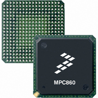
MC68360VR25VL Freescale Semiconductor, MC68360VR25VL Datasheet - Page 745

MC68360VR25VL
Manufacturer Part Number
MC68360VR25VL
Description
IC MPU QUICC 25MHZ 357-PBGA
Manufacturer
Freescale Semiconductor
Datasheets
1.MC68EN360VR25L.pdf
(14 pages)
2.MC68EN360VR25L.pdf
(2 pages)
3.MC68360AI25L.pdf
(962 pages)
Specifications of MC68360VR25VL
Processor Type
M683xx 32-Bit
Speed
25MHz
Voltage
3.3V
Mounting Type
Surface Mount
Package / Case
357-PBGA
Family Name
M68000
Device Core
ColdFire
Device Core Size
32b
Frequency (max)
25MHz
Instruction Set Architecture
RISC
Operating Supply Voltage (max)
3.3V
Operating Supply Voltage (min)
2.7V
Operating Temp Range
0C to 70C
Operating Temperature Classification
Commercial
Mounting
Surface Mount
Pin Count
357
Package Type
BGA
Lead Free Status / RoHS Status
Lead free / RoHS Compliant
Features
-
Lead Free Status / Rohs Status
Compliant
Available stocks
Company
Part Number
Manufacturer
Quantity
Price
Company:
Part Number:
MC68360VR25VL
Manufacturer:
Exar
Quantity:
160
Company:
Part Number:
MC68360VR25VL
Manufacturer:
Freescale Semiconductor
Quantity:
10 000
Company:
Part Number:
MC68360VR25VLR2
Manufacturer:
Freescale Semiconductor
Quantity:
10 000
- Current page: 745 of 962
- Download datasheet (4Mb)
The MC68302 ORx register most closely corresponds to the QUICC ORx.
TIMERS
The MC68302 contains two general-purpose timers. The QUICC contains four general-pur-
pose timers, which are the same as the MC68302 timers, but slightly enhanced. The QUICC
also contains a timer global configuration register (TGCR), which allows all four timers to be
enabled simultaneously and allows the timers to be internally cascaded into 32-bit timers.
The MC68302 TMRx register most closely corresponds to the QUICC TMRx.
The MC68302 TRRx register is the same as the QUICC TRRx.
The MC68302 TCRx register is the same as the QUICC TCRx.
BA23–BA13 that was set in A23–A13, and clear BA31–BA24 and BA12–BA11.
The three function code (FC2–FC0) bits become the four function code (FC3–FC0) bits
of the QUICC ORx.
The CFC bit is implemented as the FCM3–FCM0 bits on the QUICC ORx. This gives more
flexibility in determining the function codes that cause the chip select to activate. If the
MC68302 CFC bit was cleared, then clear FCM3–FCM0 on the QUICC. Also, to match
MC68302 behavior, clear the NCS bit in the QUICC GMR.
The MRW bit in the ORx and the RW bit in the BRx of the MC68302 simply become the
WP bit on the QUICC BRx. On the QUICC, the choice exists for asserting the chip select
for reads and writes (WP = 0) or just reads (WP = 1).
The MC68302 base address mask bits A23–A13 become the AM27–AM11 bits in the
QUICC ORx. Note that this allows both larger and smaller block sizes than what the
MC68302 provides. To transfer a block range, take bits A23–A13 of the MC68302 and
write them to AM23–AM13. Then set AM32–AM24 and clear AM12–AM11.
The three MC68302 DTACK bits become the four TCYC3–TCYC0 bits of the QUICC
ORx. Note that the maximum number of wait states is increased from 6 to 15 on the
QUICC.
The RST bit is now located in the QUICC TGCR.
The ICLK bits are still in the same location of the QUICC TMR. The bit encodings are the
same except for 00 combination, which is now implemented by the EN bit in the QUICC
TGCR.
The FRR bit is still in the same location of the QUICC TMR.
The ORI bit is still in the same location of the QUICC TMR.
The OM bit is still in the same location of the QUICC TMR, but the meaning of OM = 0
mode can be different. The active-low pulse can be longer than on the MC68302, depend-
ing on the frequency of the input clock source.
The CE bits are still in the same location of the QUICC TMR.
The PS bits are still in the same location of the QUICC TMR.
Freescale Semiconductor, Inc.
For More Information On This Product,
MC68360 USER’S MANUAL
Go to: www.freescale.com
Applications
Related parts for MC68360VR25VL
Image
Part Number
Description
Manufacturer
Datasheet
Request
R
Part Number:
Description:
Manufacturer:
Freescale Semiconductor, Inc
Datasheet:

Part Number:
Description:
MC68360 MC68360 Multiple Ethernet Channels on the QUICC
Manufacturer:
Motorola / Freescale Semiconductor

Part Number:
Description:
MC68360 Implementing an 8 bit Eprom for an MC68EC040-MC68360 System
Manufacturer:
Motorola / Freescale Semiconductor

Part Number:
Description:
MC68360 Interfacing the MC68060 to the MC68360
Manufacturer:
Motorola / Freescale Semiconductor

Part Number:
Description:
MC68360 MC68360 RAM Microcode Package Option Overview
Manufacturer:
Motorola / Freescale Semiconductor

Part Number:
Description:
MC68360 MC68360 CPM-CPU Interaction
Manufacturer:
Motorola / Freescale Semiconductor

Part Number:
Description:
MC68360 Interfacing SDRAM to the MC68360 QUICC Device
Manufacturer:
Motorola / Freescale Semiconductor

Part Number:
Description:
MC68360 Interfacing the QUICC to a MCM516400 (4Mx4 10-12 column-row) DRAM
Manufacturer:
Motorola / Freescale Semiconductor

Part Number:
Description:
MC68360 Interfacing the 68360 (QUICC) to T1-E1 Systems
Manufacturer:
Motorola / Freescale Semiconductor

Part Number:
Description:
MC68360 Multiple QUICC Design Concept
Manufacturer:
Motorola / Freescale Semiconductor
Part Number:
Description:
Manufacturer:
Freescale Semiconductor, Inc
Datasheet:
Part Number:
Description:
Manufacturer:
Freescale Semiconductor, Inc
Datasheet:
Part Number:
Description:
Manufacturer:
Freescale Semiconductor, Inc
Datasheet:
Part Number:
Description:
Manufacturer:
Freescale Semiconductor, Inc
Datasheet:
Part Number:
Description:
Manufacturer:
Freescale Semiconductor, Inc
Datasheet:


