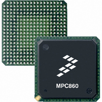
MC68360VR25VL Freescale Semiconductor, MC68360VR25VL Datasheet - Page 419

MC68360VR25VL
Manufacturer Part Number
MC68360VR25VL
Description
IC MPU QUICC 25MHZ 357-PBGA
Manufacturer
Freescale Semiconductor
Datasheets
1.MC68EN360VR25L.pdf
(14 pages)
2.MC68EN360VR25L.pdf
(2 pages)
3.MC68360AI25L.pdf
(962 pages)
Specifications of MC68360VR25VL
Processor Type
M683xx 32-Bit
Speed
25MHz
Voltage
3.3V
Mounting Type
Surface Mount
Package / Case
357-PBGA
Family Name
M68000
Device Core
ColdFire
Device Core Size
32b
Frequency (max)
25MHz
Instruction Set Architecture
RISC
Operating Supply Voltage (max)
3.3V
Operating Supply Voltage (min)
2.7V
Operating Temp Range
0C to 70C
Operating Temperature Classification
Commercial
Mounting
Surface Mount
Pin Count
357
Package Type
BGA
Lead Free Status / RoHS Status
Lead free / RoHS Compliant
Features
-
Lead Free Status / Rohs Status
Compliant
Available stocks
Company
Part Number
Manufacturer
Quantity
Price
Company:
Part Number:
MC68360VR25VL
Manufacturer:
Exar
Quantity:
160
Company:
Part Number:
MC68360VR25VL
Manufacturer:
Freescale Semiconductor
Quantity:
10 000
Company:
Part Number:
MC68360VR25VLR2
Manufacturer:
Freescale Semiconductor
Quantity:
10 000
- Current page: 419 of 962
- Download datasheet (4Mb)
the bits that are enabled by the transmitter route RAM and will three-state L1TXDx other-
wise.
7.8.6.2 IDL INTERFACE PROGRAMMING. The user can program the channels used for
the IDL bus interface to the appropriate configuration. First, the user should program the
SIMODE to the IDL grant mode for that channel, using the GMx bits. The user can program
more than one channel to interface to the IDL bus. If the receive and transmit section are
used for interfacing to the same IDL bus, the user can internally connect the receive clock
and sync signals to the SI RAM transmit section, using the CRTx bits. The user has to pro-
gram the RAM section used for the IDL channels to the desired routing. (An example is
shown in 7.8.4.6 SI RAM Programming Example.) The user should then define the IDL
frame structure to be a delay of 1 bit from frame sync to data, to falling edge sample sync,
and the clock edge to transmit on the rising edge of the clock. The L1TXDx pin should be
programmed to be three-stated when inactive (through the parallel I/O open-drain register).
To support the D channel, the user must program the appropriate GRx bit in SIMODE and
program the RAM entry to route data to that serial controller. The two definitions of IDL, 8
bits and 10 bits, are supported by only modifying the SI RAM programming. In both cases,
the L1GRx pin will be sampled with the L1TSYNCx signal and transferred to the D channel
SCC as a grant indication. The same procedure is valid for supporting an IDL bus in the sec-
ond channel.
For example, assuming the 7.8.4.6 SI RAM Programming Example, which uses SCC1,
SCC2, and SCC4, connected to the TDMx pins, with no other SCCs connected, the initial-
ization sequence is as follows:
1. Program the SI RAM. Write all entries that are not used with $0001, setting
2. SIMODE = $00000145. Only TDMa is used; the SMCs are not connected.
3. SICR = $400040C0. Only SCC4, SCC2, and SCC1 are connected to the TSA.
4. PAODR bit 6 = 1. Configures L1TXDa to an open-drain output.
the LST bit and disabling the routing function.
SCC1 supports the grant mechanism since it is on the D channel.
Since IDL requires the same routing for both receive and trans-
mit, an exact duplicate of the above entries should be written to
both the receive and transmit sections of the SI RAM beginning
at SI RAM addresses 0 and 128, respectively.
Entry
No.
1
2
3
4
5
SWTR
0
0
0
0
0
Freescale Semiconductor, Inc.
For More Information On This Product,
SSEL
0000
0000
0000
0000
0001
MC68360 USER’S MANUAL
Go to: www.freescale.com
CSEL
010
001
000
100
001
0000
0000
0000
0000
0000
CNT
NOTE
RAM Word
BYT
1
0
0
1
0
Serial Interface with Time Slot Assigner
LST
0
0
0
0
1
1 Bit SCC1 Strobe1
1 Bit No Support
description
8 Bits SCC2
8 Bits SCC4
1 Bit SCC1
Related parts for MC68360VR25VL
Image
Part Number
Description
Manufacturer
Datasheet
Request
R
Part Number:
Description:
Manufacturer:
Freescale Semiconductor, Inc
Datasheet:

Part Number:
Description:
MC68360 MC68360 Multiple Ethernet Channels on the QUICC
Manufacturer:
Motorola / Freescale Semiconductor

Part Number:
Description:
MC68360 Implementing an 8 bit Eprom for an MC68EC040-MC68360 System
Manufacturer:
Motorola / Freescale Semiconductor

Part Number:
Description:
MC68360 Interfacing the MC68060 to the MC68360
Manufacturer:
Motorola / Freescale Semiconductor

Part Number:
Description:
MC68360 MC68360 RAM Microcode Package Option Overview
Manufacturer:
Motorola / Freescale Semiconductor

Part Number:
Description:
MC68360 MC68360 CPM-CPU Interaction
Manufacturer:
Motorola / Freescale Semiconductor

Part Number:
Description:
MC68360 Interfacing SDRAM to the MC68360 QUICC Device
Manufacturer:
Motorola / Freescale Semiconductor

Part Number:
Description:
MC68360 Interfacing the QUICC to a MCM516400 (4Mx4 10-12 column-row) DRAM
Manufacturer:
Motorola / Freescale Semiconductor

Part Number:
Description:
MC68360 Interfacing the 68360 (QUICC) to T1-E1 Systems
Manufacturer:
Motorola / Freescale Semiconductor

Part Number:
Description:
MC68360 Multiple QUICC Design Concept
Manufacturer:
Motorola / Freescale Semiconductor
Part Number:
Description:
Manufacturer:
Freescale Semiconductor, Inc
Datasheet:
Part Number:
Description:
Manufacturer:
Freescale Semiconductor, Inc
Datasheet:
Part Number:
Description:
Manufacturer:
Freescale Semiconductor, Inc
Datasheet:
Part Number:
Description:
Manufacturer:
Freescale Semiconductor, Inc
Datasheet:
Part Number:
Description:
Manufacturer:
Freescale Semiconductor, Inc
Datasheet:


