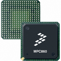
MC68360VR25VL Freescale Semiconductor, MC68360VR25VL Datasheet - Page 438

MC68360VR25VL
Manufacturer Part Number
MC68360VR25VL
Description
IC MPU QUICC 25MHZ 357-PBGA
Manufacturer
Freescale Semiconductor
Datasheets
1.MC68EN360VR25L.pdf
(14 pages)
2.MC68EN360VR25L.pdf
(2 pages)
3.MC68360AI25L.pdf
(962 pages)
Specifications of MC68360VR25VL
Processor Type
M683xx 32-Bit
Speed
25MHz
Voltage
3.3V
Mounting Type
Surface Mount
Package / Case
357-PBGA
Family Name
M68000
Device Core
ColdFire
Device Core Size
32b
Frequency (max)
25MHz
Instruction Set Architecture
RISC
Operating Supply Voltage (max)
3.3V
Operating Supply Voltage (min)
2.7V
Operating Temp Range
0C to 70C
Operating Temperature Classification
Commercial
Mounting
Surface Mount
Pin Count
357
Package Type
BGA
Lead Free Status / RoHS Status
Lead free / RoHS Compliant
Features
-
Lead Free Status / Rohs Status
Compliant
Available stocks
Company
Part Number
Manufacturer
Quantity
Price
Company:
Part Number:
MC68360VR25VL
Manufacturer:
Exar
Quantity:
160
Company:
Part Number:
MC68360VR25VL
Manufacturer:
Freescale Semiconductor
Quantity:
10 000
Company:
Part Number:
MC68360VR25VLR2
Manufacturer:
Freescale Semiconductor
Quantity:
10 000
- Current page: 438 of 962
- Download datasheet (4Mb)
Serial Communication Controllers (SCCs)
CDS—CD Sampling
CTSS—CTS Sampling
TFL—Transmit FIFO Length
RFW—Rx FIFO Width
TXSY—Transmitter Synchronized to the Receiver
7-114
The TXSY bit is particularly intended for X.21 applications where the transmitted data
must begin an exact multiple of 8-bit periods after the receive data arrives.
0 = The CD input is assumed to be asynchronous with the data. It is internally synchro-
1 = The CD input is assumed to be synchronous with the data, giving faster operation.
0 = The CTS input is assumed to be asynchronous with the data. It is internally syn-
1 = The CTS input is assumed to be synchronous with the data, giving faster operation.
0 = Normal operation. The transmit FIFO is 32 bytes for SCC1 and 16 bytes for the oth-
1 = The transmit FIFO is 1 byte. This may be used with character-oriented protocols
0 = Rx FIFO is 32-bits wide for maximum performance. Data will not normally be writ-
1 = Low-latency operation. The Rx FIFO is 8-bits wide, and the receive FIFO is one-
0 = No synchronization between receiver and transmitter (default).
1 = The transmit bit stream is synchronized to the receiver. Additionally, if RSYN = 1,
nized by the SCC, and then data is received.
In this mode, CD must transition while the receive clock is in the low state. As soon
as CD is low, data begins being received. This mode is especially useful when con-
necting QUICCs in transparent mode since it allows the RTS pin of one QUICC to
be directly connected to the CD pin of the other QUICC.
chronized by the SCC, and data is then transmitted after several serial clock de-
lays.
In this mode, CTS must transition while the transmit clock is in the low state. As
soon as CTS is low, data immediately begins transmission. This mode is especially
useful when connecting QUICCs in transparent mode since it allows the RTS pin
of one QUICC to be directly connected to the CTS pin of the other QUICC.
er SCCs.
such as UART to ensure a minimum FIFO latency at the expense of performance.
ten to receive buffers until at least 32 bits have been received. This configuration
is required for HDLC-type protocols and Ethernet; it is the recommended configu-
ration for high-performance transparent modes. In this mode, the receive FIFO is
32 bytes for SCC1 and 16 bytes for the other SCCs.
fourth its normal size (8 bytes for SCC1 and 4 bytes for the other SCCs). This al-
lows data to be written to the data buffer each time a character is received, without
waiting for 32 bits to be received. This configuration must be chosen for character-
oriented protocols such as UART and BISYNC. It may also be used for low-perfor-
mance, low-latency, totally transparent operation if desired. It must not be used
with HDLC, HDLC Bus, AppleTalk, or Ethernet, or erratic behavior may result.
then transmission in the totally transparent mode will not occur until the receiver
has synchronized with the bit stream and the CTS signal is asserted to the SCC.
Assuming CTS is already asserted, transmission will begin eight clocks after the
Freescale Semiconductor, Inc.
For More Information On This Product,
MC68360 USER’S MANUAL
Go to: www.freescale.com
Related parts for MC68360VR25VL
Image
Part Number
Description
Manufacturer
Datasheet
Request
R
Part Number:
Description:
Manufacturer:
Freescale Semiconductor, Inc
Datasheet:

Part Number:
Description:
MC68360 MC68360 Multiple Ethernet Channels on the QUICC
Manufacturer:
Motorola / Freescale Semiconductor

Part Number:
Description:
MC68360 Implementing an 8 bit Eprom for an MC68EC040-MC68360 System
Manufacturer:
Motorola / Freescale Semiconductor

Part Number:
Description:
MC68360 Interfacing the MC68060 to the MC68360
Manufacturer:
Motorola / Freescale Semiconductor

Part Number:
Description:
MC68360 MC68360 RAM Microcode Package Option Overview
Manufacturer:
Motorola / Freescale Semiconductor

Part Number:
Description:
MC68360 MC68360 CPM-CPU Interaction
Manufacturer:
Motorola / Freescale Semiconductor

Part Number:
Description:
MC68360 Interfacing SDRAM to the MC68360 QUICC Device
Manufacturer:
Motorola / Freescale Semiconductor

Part Number:
Description:
MC68360 Interfacing the QUICC to a MCM516400 (4Mx4 10-12 column-row) DRAM
Manufacturer:
Motorola / Freescale Semiconductor

Part Number:
Description:
MC68360 Interfacing the 68360 (QUICC) to T1-E1 Systems
Manufacturer:
Motorola / Freescale Semiconductor

Part Number:
Description:
MC68360 Multiple QUICC Design Concept
Manufacturer:
Motorola / Freescale Semiconductor
Part Number:
Description:
Manufacturer:
Freescale Semiconductor, Inc
Datasheet:
Part Number:
Description:
Manufacturer:
Freescale Semiconductor, Inc
Datasheet:
Part Number:
Description:
Manufacturer:
Freescale Semiconductor, Inc
Datasheet:
Part Number:
Description:
Manufacturer:
Freescale Semiconductor, Inc
Datasheet:
Part Number:
Description:
Manufacturer:
Freescale Semiconductor, Inc
Datasheet:


