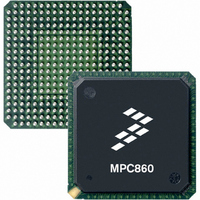
MC68360VR25VL Freescale Semiconductor, MC68360VR25VL Datasheet - Page 396

MC68360VR25VL
Manufacturer Part Number
MC68360VR25VL
Description
IC MPU QUICC 25MHZ 357-PBGA
Manufacturer
Freescale Semiconductor
Datasheets
1.MC68EN360VR25L.pdf
(14 pages)
2.MC68EN360VR25L.pdf
(2 pages)
3.MC68360AI25L.pdf
(962 pages)
Specifications of MC68360VR25VL
Processor Type
M683xx 32-Bit
Speed
25MHz
Voltage
3.3V
Mounting Type
Surface Mount
Package / Case
357-PBGA
Family Name
M68000
Device Core
ColdFire
Device Core Size
32b
Frequency (max)
25MHz
Instruction Set Architecture
RISC
Operating Supply Voltage (max)
3.3V
Operating Supply Voltage (min)
2.7V
Operating Temp Range
0C to 70C
Operating Temperature Classification
Commercial
Mounting
Surface Mount
Pin Count
357
Package Type
BGA
Lead Free Status / RoHS Status
Lead free / RoHS Compliant
Features
-
Lead Free Status / Rohs Status
Compliant
Available stocks
Company
Part Number
Manufacturer
Quantity
Price
Company:
Part Number:
MC68360VR25VL
Manufacturer:
Exar
Quantity:
160
Company:
Part Number:
MC68360VR25VL
Manufacturer:
Freescale Semiconductor
Quantity:
10 000
Company:
Part Number:
MC68360VR25VLR2
Manufacturer:
Freescale Semiconductor
Quantity:
10 000
- Current page: 396 of 962
- Download datasheet (4Mb)
Serial Interface with Time Slot Assigner
7.8.4.5 PROGRAMMING SI RAM ENTRIES. The programming of each word within the
RAM determines the routing of the serial bits (or bit groups) and the assertion of strobe out-
puts. The RAM programming codes are as follows:
Bit 15 LOOP (Loop back this time slot)
SWTR—Switch Tx and Rx
7-72
LOOP
15
The SWTR bit is only valid in the receive route RAM and is ignored in the transmit route
RAM. This bit affects the operation of both the L1RXD and L1TXD pins
The SWTR bit would only be set in a special situation where the user desires to receive
data from a transmit pin and transmit data on a receive pin. For instance, consider the sit-
uation where devices A and B are connected to the same TDM, each with different time
slots. Normally, there is no opportunity for stations A and B to communicate with each oth-
er directly over the TDM, since they both receive the same TDM receive data and transmit
on the same TDM transmit signal (see Figure 7-27).
NOTES:
1: Only available on REV C mask or later. NOT Available on REV A or B.
Rev A mask is C63T
Rev B mask are C69T, and F35G
Current Rev C mask are E63C, E68C and F15W
1
0 = normal mode
1 = loop back mode for this time slot
SI RAM ADDRESS: 0
SWTR
14
(16-BITS WIDE)
13
128
158
30
SSEL1–SSEL4
12
Figure 7-26. Two TDMs with Dynamic Frames
16 ENTRIES
16 ENTRIES
16 ENTRIES
16 ENTRIES
ROUTE
ROUTE
ROUTE
ROUTE
RXa
RXa
TXa
TXa
11
Freescale Semiconductor, Inc.
For More Information On This Product,
10
MC68360 USER’S MANUAL
160
32
62
Go to: www.freescale.com
TWO CHANNELS WITH SHADOW RAM
190
—
FOR DYNAMIC ROUTE CHANGE
9
L1RCLKa
FRAMING SIGNALS
L1RSYNCa
L1TCLKa
L1TSYNCa
8
RDM = 11
CSEL
7
222
192
64
94
6
16 ENTRIES
16 ENTRIES
16 ENTRIES
16 ENTRIES
ROUTE
ROUTE
ROUTE
ROUTE
TXb
TXb
RXb
RXb
5
4
CNT
126
224
96
254
3
FRAMING SIGNALS
L1RCLKb
L1RSYNCb
L1TCLKb
L1TSYNCb
2
BYT
1
LST
0
Related parts for MC68360VR25VL
Image
Part Number
Description
Manufacturer
Datasheet
Request
R
Part Number:
Description:
Manufacturer:
Freescale Semiconductor, Inc
Datasheet:

Part Number:
Description:
MC68360 MC68360 Multiple Ethernet Channels on the QUICC
Manufacturer:
Motorola / Freescale Semiconductor

Part Number:
Description:
MC68360 Implementing an 8 bit Eprom for an MC68EC040-MC68360 System
Manufacturer:
Motorola / Freescale Semiconductor

Part Number:
Description:
MC68360 Interfacing the MC68060 to the MC68360
Manufacturer:
Motorola / Freescale Semiconductor

Part Number:
Description:
MC68360 MC68360 RAM Microcode Package Option Overview
Manufacturer:
Motorola / Freescale Semiconductor

Part Number:
Description:
MC68360 MC68360 CPM-CPU Interaction
Manufacturer:
Motorola / Freescale Semiconductor

Part Number:
Description:
MC68360 Interfacing SDRAM to the MC68360 QUICC Device
Manufacturer:
Motorola / Freescale Semiconductor

Part Number:
Description:
MC68360 Interfacing the QUICC to a MCM516400 (4Mx4 10-12 column-row) DRAM
Manufacturer:
Motorola / Freescale Semiconductor

Part Number:
Description:
MC68360 Interfacing the 68360 (QUICC) to T1-E1 Systems
Manufacturer:
Motorola / Freescale Semiconductor

Part Number:
Description:
MC68360 Multiple QUICC Design Concept
Manufacturer:
Motorola / Freescale Semiconductor
Part Number:
Description:
Manufacturer:
Freescale Semiconductor, Inc
Datasheet:
Part Number:
Description:
Manufacturer:
Freescale Semiconductor, Inc
Datasheet:
Part Number:
Description:
Manufacturer:
Freescale Semiconductor, Inc
Datasheet:
Part Number:
Description:
Manufacturer:
Freescale Semiconductor, Inc
Datasheet:
Part Number:
Description:
Manufacturer:
Freescale Semiconductor, Inc
Datasheet:


