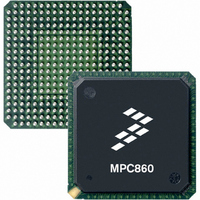
MC68360VR25VL Freescale Semiconductor, MC68360VR25VL Datasheet - Page 138

MC68360VR25VL
Manufacturer Part Number
MC68360VR25VL
Description
IC MPU QUICC 25MHZ 357-PBGA
Manufacturer
Freescale Semiconductor
Datasheets
1.MC68EN360VR25L.pdf
(14 pages)
2.MC68EN360VR25L.pdf
(2 pages)
3.MC68360AI25L.pdf
(962 pages)
Specifications of MC68360VR25VL
Processor Type
M683xx 32-Bit
Speed
25MHz
Voltage
3.3V
Mounting Type
Surface Mount
Package / Case
357-PBGA
Family Name
M68000
Device Core
ColdFire
Device Core Size
32b
Frequency (max)
25MHz
Instruction Set Architecture
RISC
Operating Supply Voltage (max)
3.3V
Operating Supply Voltage (min)
2.7V
Operating Temp Range
0C to 70C
Operating Temperature Classification
Commercial
Mounting
Surface Mount
Pin Count
357
Package Type
BGA
Lead Free Status / RoHS Status
Lead free / RoHS Compliant
Features
-
Lead Free Status / Rohs Status
Compliant
Available stocks
Company
Part Number
Manufacturer
Quantity
Price
Company:
Part Number:
MC68360VR25VL
Manufacturer:
Exar
Quantity:
160
Company:
Part Number:
MC68360VR25VL
Manufacturer:
Freescale Semiconductor
Quantity:
10 000
Company:
Part Number:
MC68360VR25VLR2
Manufacturer:
Freescale Semiconductor
Quantity:
10 000
- Current page: 138 of 962
- Download datasheet (4Mb)
Freescale Semiconductor, Inc.
Bus Operation
4.6.8 Show Cycles
The QUICC can perform data transfers with its internal modules without using the external
bus, but when debugging, it is desirable to have address and data information appear on the
external bus. These external bus cycles, called show cycles, are distinguished by the fact
that AS is not asserted externally. DS is used to signal address strobe timing in show cycles.
After reset, show cycles are disabled and must be enabled by writing to the SHEN bits in the
module configuration register. When show cycles are disabled, the address bus, function
codes, size, and read/write signals continue to reflect internal bus activity. However, AS and
DS are not asserted externally, and the external data bus remains in a high impedance
state. When show cycles are enabled, DS indicates address strobe timing and the external
data bus contains data. The following paragraphs are a state-by-state description of show
cycles, and Figure 4-45 illustrates a show cycle timing diagram. Refer to Section 10 Electri-
cal Characteristics for specific timing information.
State 0 – During state 0, the address and function codes become valid, R/W is driven to indi-
cate a show read or write cycle, and the size pins indicate the number of bytes to transfer.
During a read, the addressed peripheral is driving the data bus, and the user must take care
to avoid bus conflicts.
State 41 – One-half clock cycle later, DS (rather than AS) is asserted to indicate that address
information is valid.
State 42– No action occurs in state 42. The bus controller remains in state 42 (wait states
will be inserted) until the internal read cycle is complete.
State 43– When DS is negated, show data is valid on the next falling edge of the system
clock. The external data bus drivers are enabled so that data becomes valid on the external
bus as soon as it is available on the internal bus.
State 0 – The address, function codes, read/write, and size pins change to begin the next
cycle. Data from the preceding cycle is valid through state 0.
4-62
MC68360 USER’S MANUAL
For More Information On This Product,
Go to: www.freescale.com
Related parts for MC68360VR25VL
Image
Part Number
Description
Manufacturer
Datasheet
Request
R
Part Number:
Description:
Manufacturer:
Freescale Semiconductor, Inc
Datasheet:

Part Number:
Description:
MC68360 MC68360 Multiple Ethernet Channels on the QUICC
Manufacturer:
Motorola / Freescale Semiconductor

Part Number:
Description:
MC68360 Implementing an 8 bit Eprom for an MC68EC040-MC68360 System
Manufacturer:
Motorola / Freescale Semiconductor

Part Number:
Description:
MC68360 Interfacing the MC68060 to the MC68360
Manufacturer:
Motorola / Freescale Semiconductor

Part Number:
Description:
MC68360 MC68360 RAM Microcode Package Option Overview
Manufacturer:
Motorola / Freescale Semiconductor

Part Number:
Description:
MC68360 MC68360 CPM-CPU Interaction
Manufacturer:
Motorola / Freescale Semiconductor

Part Number:
Description:
MC68360 Interfacing SDRAM to the MC68360 QUICC Device
Manufacturer:
Motorola / Freescale Semiconductor

Part Number:
Description:
MC68360 Interfacing the QUICC to a MCM516400 (4Mx4 10-12 column-row) DRAM
Manufacturer:
Motorola / Freescale Semiconductor

Part Number:
Description:
MC68360 Interfacing the 68360 (QUICC) to T1-E1 Systems
Manufacturer:
Motorola / Freescale Semiconductor

Part Number:
Description:
MC68360 Multiple QUICC Design Concept
Manufacturer:
Motorola / Freescale Semiconductor
Part Number:
Description:
Manufacturer:
Freescale Semiconductor, Inc
Datasheet:
Part Number:
Description:
Manufacturer:
Freescale Semiconductor, Inc
Datasheet:
Part Number:
Description:
Manufacturer:
Freescale Semiconductor, Inc
Datasheet:
Part Number:
Description:
Manufacturer:
Freescale Semiconductor, Inc
Datasheet:
Part Number:
Description:
Manufacturer:
Freescale Semiconductor, Inc
Datasheet:


