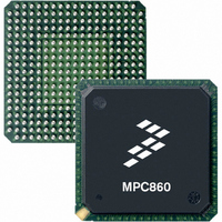
MC68360VR25VL Freescale Semiconductor, MC68360VR25VL Datasheet - Page 431

MC68360VR25VL
Manufacturer Part Number
MC68360VR25VL
Description
IC MPU QUICC 25MHZ 357-PBGA
Manufacturer
Freescale Semiconductor
Datasheets
1.MC68EN360VR25L.pdf
(14 pages)
2.MC68EN360VR25L.pdf
(2 pages)
3.MC68360AI25L.pdf
(962 pages)
Specifications of MC68360VR25VL
Processor Type
M683xx 32-Bit
Speed
25MHz
Voltage
3.3V
Mounting Type
Surface Mount
Package / Case
357-PBGA
Family Name
M68000
Device Core
ColdFire
Device Core Size
32b
Frequency (max)
25MHz
Instruction Set Architecture
RISC
Operating Supply Voltage (max)
3.3V
Operating Supply Voltage (min)
2.7V
Operating Temp Range
0C to 70C
Operating Temperature Classification
Commercial
Mounting
Surface Mount
Pin Count
357
Package Type
BGA
Lead Free Status / RoHS Status
Lead free / RoHS Compliant
Features
-
Lead Free Status / Rohs Status
Compliant
Available stocks
Company
Part Number
Manufacturer
Quantity
Price
Company:
Part Number:
MC68360VR25VL
Manufacturer:
Exar
Quantity:
160
Company:
Part Number:
MC68360VR25VL
Manufacturer:
Freescale Semiconductor
Quantity:
10 000
Company:
Part Number:
MC68360VR25VLR2
Manufacturer:
Freescale Semiconductor
Quantity:
10 000
- Current page: 431 of 962
- Download datasheet (4Mb)
RST—Reset BRG
EN—Enable BRG Count
EXTC1–EXTC0—External Clock Source
ATB—Autobaud
CD11–CD0—Clock Divider
This bit performs a software reset of the BRG identical to that of an external reset. A reset
disables the BRG and sets the BRGO output clock. (This can only be seen externally if
the BRGO function is enabled to reach the corresponding port B parallel I/O pin.)
This bit is used to dynamically stop the BRG from counting, which may be useful for low-
power modes.
The EXTC bits select the BRG input clock from the internal BRGCLK or one of three ex-
ternal pins.
When set, this bit selects autobaud operation of the BRG on the corresponding RXDx pin.
The clock divider bits, CD11–CD0, and the prescaler determine the BRG output clock
rate. CD11–CD0 are used to preset a 12-bit counter that is decremented at the prescaler
output rate. The counter is not accessible to the user. When the counter reaches zero, it
is reloaded from the clock divider bits. Thus, a value of $FFF in CD11–CD0 produces the
minimum clock rate (divide by 4096), and a value of $0000 produces the maximum clock
rate (divide by 1).
Even when dividing by an odd number, the counter ensures a 50% duty cycle by asserting
the terminal count once on clock low and next on clock high. The terminal count signals
counter expiration and toggles the clock.
0 = Enable the BRG.
1 = Reset the BRG (software reset).
0 = Stop all clocks to the BRG.
1 = Enable clocks to the BRG.
00 = The BRG input clock comes from the BRGCLK (internal clock generated by the
01 = The BRG input clock comes from the CLK2 pin.
10 = The BRG input clock comes from the CLK6 pin.
11 = Reserved.
0 = Normal operation of the BRG.
1 = When RXDx goes low, the BRG will determine the length of the start bit and syn-
chronize the BRG to the actual baud rate.
clock synthesizer in the SIM60).
This bit must remain clear (0) until the SCC receives 3 Rx clocks,
then the user must set this bit to one in order to obtain the correct
baud rate. When the baud rate is obtained and locked it will be
indicated by setting the AB bit in the UART event register.
Freescale Semiconductor, Inc.
For More Information On This Product,
MC68360 USER’S MANUAL
Go to: www.freescale.com
NOTE
Baud Rate Generators (BRGs)
Related parts for MC68360VR25VL
Image
Part Number
Description
Manufacturer
Datasheet
Request
R
Part Number:
Description:
Manufacturer:
Freescale Semiconductor, Inc
Datasheet:

Part Number:
Description:
MC68360 MC68360 Multiple Ethernet Channels on the QUICC
Manufacturer:
Motorola / Freescale Semiconductor

Part Number:
Description:
MC68360 Implementing an 8 bit Eprom for an MC68EC040-MC68360 System
Manufacturer:
Motorola / Freescale Semiconductor

Part Number:
Description:
MC68360 Interfacing the MC68060 to the MC68360
Manufacturer:
Motorola / Freescale Semiconductor

Part Number:
Description:
MC68360 MC68360 RAM Microcode Package Option Overview
Manufacturer:
Motorola / Freescale Semiconductor

Part Number:
Description:
MC68360 MC68360 CPM-CPU Interaction
Manufacturer:
Motorola / Freescale Semiconductor

Part Number:
Description:
MC68360 Interfacing SDRAM to the MC68360 QUICC Device
Manufacturer:
Motorola / Freescale Semiconductor

Part Number:
Description:
MC68360 Interfacing the QUICC to a MCM516400 (4Mx4 10-12 column-row) DRAM
Manufacturer:
Motorola / Freescale Semiconductor

Part Number:
Description:
MC68360 Interfacing the 68360 (QUICC) to T1-E1 Systems
Manufacturer:
Motorola / Freescale Semiconductor

Part Number:
Description:
MC68360 Multiple QUICC Design Concept
Manufacturer:
Motorola / Freescale Semiconductor
Part Number:
Description:
Manufacturer:
Freescale Semiconductor, Inc
Datasheet:
Part Number:
Description:
Manufacturer:
Freescale Semiconductor, Inc
Datasheet:
Part Number:
Description:
Manufacturer:
Freescale Semiconductor, Inc
Datasheet:
Part Number:
Description:
Manufacturer:
Freescale Semiconductor, Inc
Datasheet:
Part Number:
Description:
Manufacturer:
Freescale Semiconductor, Inc
Datasheet:


