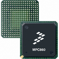
MC68360VR25VL Freescale Semiconductor, MC68360VR25VL Datasheet - Page 87

MC68360VR25VL
Manufacturer Part Number
MC68360VR25VL
Description
IC MPU QUICC 25MHZ 357-PBGA
Manufacturer
Freescale Semiconductor
Datasheets
1.MC68EN360VR25L.pdf
(14 pages)
2.MC68EN360VR25L.pdf
(2 pages)
3.MC68360AI25L.pdf
(962 pages)
Specifications of MC68360VR25VL
Processor Type
M683xx 32-Bit
Speed
25MHz
Voltage
3.3V
Mounting Type
Surface Mount
Package / Case
357-PBGA
Family Name
M68000
Device Core
ColdFire
Device Core Size
32b
Frequency (max)
25MHz
Instruction Set Architecture
RISC
Operating Supply Voltage (max)
3.3V
Operating Supply Voltage (min)
2.7V
Operating Temp Range
0C to 70C
Operating Temperature Classification
Commercial
Mounting
Surface Mount
Pin Count
357
Package Type
BGA
Lead Free Status / RoHS Status
Lead free / RoHS Compliant
Features
-
Lead Free Status / Rohs Status
Compliant
Available stocks
Company
Part Number
Manufacturer
Quantity
Price
Company:
Part Number:
MC68360VR25VL
Manufacturer:
Exar
Quantity:
160
Company:
Part Number:
MC68360VR25VL
Manufacturer:
Freescale Semiconductor
Quantity:
10 000
Company:
Part Number:
MC68360VR25VLR2
Manufacturer:
Freescale Semiconductor
Quantity:
10 000
- Current page: 87 of 962
- Download datasheet (4Mb)
Figure 4-6 shows a word transfer to an 8-bit bus port. Like the preceding example, this
example requires two bus cycles. Each bus cycle transfers a single byte. The size signals
for the first cycle specify two bytes; for the second cycle, they specify one byte. Figure 4-7
shows the associated bus transfer signal timing.
4.2.2 Misaligned Operands
Since operands may reside at any byte boundaries, they may be misaligned. A byte operand
is properly aligned at any address; a word operand is misaligned at an odd address; a long
word is misaligned at an address that is not evenly divisible by four. The MC68302,
MC68000/MC68008, MC68010, and MC68340 implementations allow long-word transfers
on odd-word boundaries but force exceptions if word or long-word operand transfers are
attempted at odd-byte addresses. Although the QUICC does not enforce any alignment
restrictions for data operands (including PC relative data addresses), some performance
degradation occurs when additional bus cycles are required for long-word or word operands
Figure 4-5. Long-Word Operand Write Timing (16-Bit Data Port)
FC3–FC0
D23–D16
D31–D24
DSACK0
DSACK1
A31–A2
CLKO1
SIZ0
SIZ1
R/W
AS
DS
A0
A1
Freescale Semiconductor, Inc.
For More Information On This Product,
S0
MC68360 USER’S MANUAL
Go to: www.freescale.com
WORD WRITE
S2
LONG-WORD OPERAND WRITE TO 16-BIT PORT
0P0
0P1
S4
S0
WORD WRITE
S2
0P3
0P2
S4
Bus Operation
Related parts for MC68360VR25VL
Image
Part Number
Description
Manufacturer
Datasheet
Request
R
Part Number:
Description:
Manufacturer:
Freescale Semiconductor, Inc
Datasheet:

Part Number:
Description:
MC68360 MC68360 Multiple Ethernet Channels on the QUICC
Manufacturer:
Motorola / Freescale Semiconductor

Part Number:
Description:
MC68360 Implementing an 8 bit Eprom for an MC68EC040-MC68360 System
Manufacturer:
Motorola / Freescale Semiconductor

Part Number:
Description:
MC68360 Interfacing the MC68060 to the MC68360
Manufacturer:
Motorola / Freescale Semiconductor

Part Number:
Description:
MC68360 MC68360 RAM Microcode Package Option Overview
Manufacturer:
Motorola / Freescale Semiconductor

Part Number:
Description:
MC68360 MC68360 CPM-CPU Interaction
Manufacturer:
Motorola / Freescale Semiconductor

Part Number:
Description:
MC68360 Interfacing SDRAM to the MC68360 QUICC Device
Manufacturer:
Motorola / Freescale Semiconductor

Part Number:
Description:
MC68360 Interfacing the QUICC to a MCM516400 (4Mx4 10-12 column-row) DRAM
Manufacturer:
Motorola / Freescale Semiconductor

Part Number:
Description:
MC68360 Interfacing the 68360 (QUICC) to T1-E1 Systems
Manufacturer:
Motorola / Freescale Semiconductor

Part Number:
Description:
MC68360 Multiple QUICC Design Concept
Manufacturer:
Motorola / Freescale Semiconductor
Part Number:
Description:
Manufacturer:
Freescale Semiconductor, Inc
Datasheet:
Part Number:
Description:
Manufacturer:
Freescale Semiconductor, Inc
Datasheet:
Part Number:
Description:
Manufacturer:
Freescale Semiconductor, Inc
Datasheet:
Part Number:
Description:
Manufacturer:
Freescale Semiconductor, Inc
Datasheet:
Part Number:
Description:
Manufacturer:
Freescale Semiconductor, Inc
Datasheet:


