R5F21238DFP#U0 Renesas Electronics America, R5F21238DFP#U0 Datasheet - Page 502
R5F21238DFP#U0
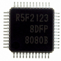
Manufacturer Part Number
R5F21238DFP#U0
Description
IC R8C/23 MCU FLASH 48-LQFP
Manufacturer
Renesas Electronics America
Series
R8C/2x/23r
Specifications of R5F21238DFP#U0
Core Size
16/32-Bit
Program Memory Size
64KB (64K x 8)
Peripherals
POR, Voltage Detect, WDT
Core Processor
R8C
Speed
20MHz
Connectivity
CAN, I²C, LIN, SIO, SSU, UART/USART
Number Of I /o
41
Program Memory Type
FLASH
Ram Size
3K x 8
Voltage - Supply (vcc/vdd)
2.7 V ~ 5.5 V
Data Converters
A/D 12x10b
Oscillator Type
Internal
Operating Temperature
-40°C ~ 85°C
Package / Case
48-LQFP
No. Of I/o's
41
Ram Memory Size
3KB
Cpu Speed
20MHz
No. Of Timers
4
Digital Ic Case Style
LQFP
Embedded Interface Type
CAN, I2C, UART
Rohs Compliant
Yes
Cpu Family
R8C
Device Core Size
16b
Frequency (max)
20MHz
Interface Type
I2C/UART
Total Internal Ram Size
3KB
# I/os (max)
41
Number Of Timers - General Purpose
5
Operating Supply Voltage (typ)
3.3/5V
Operating Supply Voltage (max)
5.5V
Operating Supply Voltage (min)
3V
On-chip Adc
12-chx10-bit
Instruction Set Architecture
CISC
Operating Temp Range
-40C to 85C
Operating Temperature Classification
Industrial
Mounting
Surface Mount
Pin Count
48
Package Type
LQFP
Lead Free Status / RoHS Status
Lead free / RoHS Compliant
For Use With
RCDK8C - KIT DEV EVAL FOR CAN R8C/23R0K521237S000BE - KIT DEV RSK R8C/23R0E521237CPE00 - EMULATOR COMPACT R8C/20/21/22/23
Eeprom Size
-
Lead Free Status / Rohs Status
Compliant
Available stocks
Company
Part Number
Manufacturer
Quantity
Price


R8C/22 Group, R8C/23 Group
Rev.2.00 Aug 20, 2008
REJ09B0251-0200
Figure 22.6
•
Select with the CMD1 to CMD0 bits for the data transfer timing from the buffer register to the general
register. However, transfer with the following timing in spite of the value of the CMD1 to CMD0 bits for
the following cases:
Value in buffer register ≥ Value in TRDGRA0 register:
Transfer at the underflow in the TRD1 register.
And then, when setting the buffer register to 0001h or above and the smaller value than the one in the
TRDGRA0 register, and the TRD1 register underflows in the fist time after setting, the value is transferred
to the general register. After that, transfer the value with the timing selected by the CMD1 to CMD0 bits.
TRDGRD0 register
TRDGRB0 register
TRDIOD0 output
TRDIOB0 output
Operation When Value in Buffer Register ≥ Value in TRDGRA0 Register in
Complementary PWM Mode
The above applies to the following conditions:
• The CMD1 to CMD0 bits in the TRDFCR register are set to 11b.
• Both the OSL0 and OLS1 bits in the TRDFCR are set to 1. (active ‘H” for normal-phase and counter-phase)
(Data in the buffer register is transferred at the compare match in the TRD0 and TRDGRA0 registers in complementary
PWM mode.)
Transfer with timing set by
CMD1 to CMD0 bits
m + 1
0000h
n3
n2
n1
Page 480 of 501
Transfer
n2
n1
n2
Transfer by
underflow in TRD1
register because of
n3 > m
n3
Transfer
n3
Transfer by
underflow in TRD1
register because
of first setting to
n2 < m
Transfer
n2
m: Setting Value in TRDGRA0 Register
n2
n1
Transfer with timing set by
CMD1 to CMD0 bits
Transfer
n1
Count value in TRD0
register
Count value in TRD1
register
22. Usage Notes
Related parts for R5F21238DFP#U0
Image
Part Number
Description
Manufacturer
Datasheet
Request
R

Part Number:
Description:
KIT STARTER FOR M16C/29
Manufacturer:
Renesas Electronics America
Datasheet:

Part Number:
Description:
KIT STARTER FOR R8C/2D
Manufacturer:
Renesas Electronics America
Datasheet:

Part Number:
Description:
R0K33062P STARTER KIT
Manufacturer:
Renesas Electronics America
Datasheet:

Part Number:
Description:
KIT STARTER FOR R8C/23 E8A
Manufacturer:
Renesas Electronics America
Datasheet:

Part Number:
Description:
KIT STARTER FOR R8C/25
Manufacturer:
Renesas Electronics America
Datasheet:

Part Number:
Description:
KIT STARTER H8S2456 SHARPE DSPLY
Manufacturer:
Renesas Electronics America
Datasheet:

Part Number:
Description:
KIT STARTER FOR R8C38C
Manufacturer:
Renesas Electronics America
Datasheet:

Part Number:
Description:
KIT STARTER FOR R8C35C
Manufacturer:
Renesas Electronics America
Datasheet:

Part Number:
Description:
KIT STARTER FOR R8CL3AC+LCD APPS
Manufacturer:
Renesas Electronics America
Datasheet:
Part Number:
Description:
KIT STARTER FOR RX610
Manufacturer:
Renesas Electronics America
Datasheet:

Part Number:
Description:
KIT STARTER FOR R32C/118
Manufacturer:
Renesas Electronics America
Datasheet:

Part Number:
Description:
KIT DEV RSK-R8C/26-29
Manufacturer:
Renesas Electronics America
Datasheet:

Part Number:
Description:
KIT STARTER FOR SH7124
Manufacturer:
Renesas Electronics America
Datasheet:

Part Number:
Description:
KIT STARTER FOR H8SX/1622
Manufacturer:
Renesas Electronics America
Datasheet:

Part Number:
Description:
KIT DEV FOR SH7203
Manufacturer:
Renesas Electronics America
Datasheet: