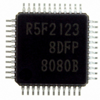
R5F21238DFP#U0 Renesas Electronics America, R5F21238DFP#U0 Datasheet - Page 188

R5F21238DFP#U0
Manufacturer Part Number
R5F21238DFP#U0
Description
IC R8C/23 MCU FLASH 48-LQFP
Manufacturer
Renesas Electronics America
Series
R8C/2x/23r
Specifications of R5F21238DFP#U0
Core Size
16/32-Bit
Program Memory Size
64KB (64K x 8)
Peripherals
POR, Voltage Detect, WDT
Core Processor
R8C
Speed
20MHz
Connectivity
CAN, I²C, LIN, SIO, SSU, UART/USART
Number Of I /o
41
Program Memory Type
FLASH
Ram Size
3K x 8
Voltage - Supply (vcc/vdd)
2.7 V ~ 5.5 V
Data Converters
A/D 12x10b
Oscillator Type
Internal
Operating Temperature
-40°C ~ 85°C
Package / Case
48-LQFP
No. Of I/o's
41
Ram Memory Size
3KB
Cpu Speed
20MHz
No. Of Timers
4
Digital Ic Case Style
LQFP
Embedded Interface Type
CAN, I2C, UART
Rohs Compliant
Yes
Cpu Family
R8C
Device Core Size
16b
Frequency (max)
20MHz
Interface Type
I2C/UART
Total Internal Ram Size
3KB
# I/os (max)
41
Number Of Timers - General Purpose
5
Operating Supply Voltage (typ)
3.3/5V
Operating Supply Voltage (max)
5.5V
Operating Supply Voltage (min)
3V
On-chip Adc
12-chx10-bit
Instruction Set Architecture
CISC
Operating Temp Range
-40C to 85C
Operating Temperature Classification
Industrial
Mounting
Surface Mount
Pin Count
48
Package Type
LQFP
Lead Free Status / RoHS Status
Lead free / RoHS Compliant
For Use With
RCDK8C - KIT DEV EVAL FOR CAN R8C/23R0K521237S000BE - KIT DEV RSK R8C/23R0E521237CPE00 - EMULATOR COMPACT R8C/20/21/22/23
Eeprom Size
-
Lead Free Status / Rohs Status
Compliant
Available stocks
Company
Part Number
Manufacturer
Quantity
Price
- Current page: 188 of 551
- Download datasheet (6Mb)
R8C/22 Group, R8C/23 Group
Rev.2.00 Aug 20, 2008
REJ09B0251-0200
Figure 14.25
14.2.5.2
The following three workarounds should be performed in programmable waveform generation mode.
(1) To write to registers TRBPRE and TRBPR during count operation (TCSTF bit is set to 1), note the
•
•
(2) To change registers TRBPRE and TRBPR during count operation (TCSTF bit is set to 1), synchronize
•
When the TRBPRE register is written continuously, allow three or more cycles of the count source for each
write interval.
When the TRBPR register is written continuously, allow three or more cycles of the prescaler underflow
for each write interval.
Workaround example (a):
As shown in Figure 14.25, write to registers TRBSC and TRBPR in the timer RB interrupt routine. These
write operations must be completed by the beginning of period A.
following points:
the TRBO output cycle using a timer RB interrupt, etc. This operation should be preformed only once in
the same output cycle. Also, make sure that writing to the TRBPR register does not occur during period
A shown in Figures 14.25 and 14.26.
The following shows the detailed workaround examples.
Programmable waveform generation mode
Workaround Example (a) When Timer RB Interrupt is Used
TRBO pin output
(a) Period between interrupt request generation and the completion of execution of an instruction. The length of time
(b) 20 cycles. 21 cycles for address match and single-step interrupts.
underflow signal
varies depending on the instruction being executed.
The DIVX instruction requires the longest time, 30 cycles (assuming no wait states and that a register is set as
the divisor).
TRBIC register
Count source/
Interrupt request
is generated
prescaler
Page 166 of 501
IR bit in
(a)
sequence
Interrupt
(b)
Primary period
Interrupt request is
acknowledged
interrupt routine
Instruction in
Set the secondary and then
the primary register immediately
Ensure sufficient time
Secondary period
Period A
14. Timers
Related parts for R5F21238DFP#U0
Image
Part Number
Description
Manufacturer
Datasheet
Request
R

Part Number:
Description:
KIT STARTER FOR M16C/29
Manufacturer:
Renesas Electronics America
Datasheet:

Part Number:
Description:
KIT STARTER FOR R8C/2D
Manufacturer:
Renesas Electronics America
Datasheet:

Part Number:
Description:
R0K33062P STARTER KIT
Manufacturer:
Renesas Electronics America
Datasheet:

Part Number:
Description:
KIT STARTER FOR R8C/23 E8A
Manufacturer:
Renesas Electronics America
Datasheet:

Part Number:
Description:
KIT STARTER FOR R8C/25
Manufacturer:
Renesas Electronics America
Datasheet:

Part Number:
Description:
KIT STARTER H8S2456 SHARPE DSPLY
Manufacturer:
Renesas Electronics America
Datasheet:

Part Number:
Description:
KIT STARTER FOR R8C38C
Manufacturer:
Renesas Electronics America
Datasheet:

Part Number:
Description:
KIT STARTER FOR R8C35C
Manufacturer:
Renesas Electronics America
Datasheet:

Part Number:
Description:
KIT STARTER FOR R8CL3AC+LCD APPS
Manufacturer:
Renesas Electronics America
Datasheet:

Part Number:
Description:
KIT STARTER FOR RX610
Manufacturer:
Renesas Electronics America
Datasheet:

Part Number:
Description:
KIT STARTER FOR R32C/118
Manufacturer:
Renesas Electronics America
Datasheet:

Part Number:
Description:
KIT DEV RSK-R8C/26-29
Manufacturer:
Renesas Electronics America
Datasheet:

Part Number:
Description:
KIT STARTER FOR SH7124
Manufacturer:
Renesas Electronics America
Datasheet:

Part Number:
Description:
KIT STARTER FOR H8SX/1622
Manufacturer:
Renesas Electronics America
Datasheet:

Part Number:
Description:
KIT DEV FOR SH7203
Manufacturer:
Renesas Electronics America
Datasheet:


