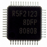
R5F21238DFP#U0 Renesas Electronics America, R5F21238DFP#U0 Datasheet - Page 379

R5F21238DFP#U0
Manufacturer Part Number
R5F21238DFP#U0
Description
IC R8C/23 MCU FLASH 48-LQFP
Manufacturer
Renesas Electronics America
Series
R8C/2x/23r
Specifications of R5F21238DFP#U0
Core Size
16/32-Bit
Program Memory Size
64KB (64K x 8)
Peripherals
POR, Voltage Detect, WDT
Core Processor
R8C
Speed
20MHz
Connectivity
CAN, I²C, LIN, SIO, SSU, UART/USART
Number Of I /o
41
Program Memory Type
FLASH
Ram Size
3K x 8
Voltage - Supply (vcc/vdd)
2.7 V ~ 5.5 V
Data Converters
A/D 12x10b
Oscillator Type
Internal
Operating Temperature
-40°C ~ 85°C
Package / Case
48-LQFP
No. Of I/o's
41
Ram Memory Size
3KB
Cpu Speed
20MHz
No. Of Timers
4
Digital Ic Case Style
LQFP
Embedded Interface Type
CAN, I2C, UART
Rohs Compliant
Yes
Cpu Family
R8C
Device Core Size
16b
Frequency (max)
20MHz
Interface Type
I2C/UART
Total Internal Ram Size
3KB
# I/os (max)
41
Number Of Timers - General Purpose
5
Operating Supply Voltage (typ)
3.3/5V
Operating Supply Voltage (max)
5.5V
Operating Supply Voltage (min)
3V
On-chip Adc
12-chx10-bit
Instruction Set Architecture
CISC
Operating Temp Range
-40C to 85C
Operating Temperature Classification
Industrial
Mounting
Surface Mount
Pin Count
48
Package Type
LQFP
Lead Free Status / RoHS Status
Lead free / RoHS Compliant
For Use With
RCDK8C - KIT DEV EVAL FOR CAN R8C/23R0K521237S000BE - KIT DEV RSK R8C/23R0E521237CPE00 - EMULATOR COMPACT R8C/20/21/22/23
Eeprom Size
-
Lead Free Status / Rohs Status
Compliant
Available stocks
Company
Part Number
Manufacturer
Quantity
Price
- Current page: 379 of 551
- Download datasheet (6Mb)
R8C/22 Group, R8C/23 Group
Rev.2.00 Aug 20, 2008
REJ09B0251-0200
17.3
Figure 17.2
LIN Control Register
The hardware LIN contains the following registers.
Figure 17.2 and Figure 17.3 show the LINCR and LINST Registers.
b7 b6 b5 b4
NOTES:
•
•
1.
2.
3. Input to timer RA and UART0 are prohibited immediately after the LINE bit is set to 1(Causes LIN to start operating).
LIN Control Register (LINCR)
LIN Status Register (LINST)
Register Configuration
After setting the LSTART bit, confirm that the RXDSF flag is set to 1 before Synch Break input starts.
Before changing LIN operation modes, temporarily stop the LIN operation (LINE bit = 0).
Refer to Figure 17.5 Exam ple of Header Field Transm ission Flow chart (1) and Figure 17.9 Exam ple of
Header Field Reception Flow chart (2).
b3 b2 b1 b0
LINCR Register
Bit Symbol
LSTART
Symbol
RXDSF
LINCR
SFIE
SBIE
BCIE
MST
Page 357 of 501
SBE
LINE
Synch Field measurement-
completed interrupt enable bit
Synch Break detection interrupt
enable bit
Bus collision detection interrupt
enable bit
RxD0 input status flag
Synch Break detection start bit
RxD0 input unmasking timing
select bit
(effective in only slave mode)
LIN operation mode setting bit
LIN operation start bit
Address
Bit Name
0106h
(2)
(1)
0 : Disables Synch Field measurement-
1 : Enables Synch Field measurement-
0 : Disables Synch Break detection interrupt
1 : Enables Synch Break detection interrupt
0 : Disables bus collision detection interrupt
1 : Enables bus collision detection interrupt
0 : RXD0 input enabled
1 : RXD0 input disabled
When this bit is set to 1, Timer RA input is
enabled and RXD0 input is disabled.
When read, its content is 0.
0 : Unmasked after Synch Break is detected
1 : Unmasked after Synch Field measurement
0 : Slave mode
1 : Master mode
0 : Causes LIN to stop
1 : Causes LIN to start operating
completed interrupt
completed interrupt
is completed
(Synch Break detection circuit actuated)
(timer RA output OR’ed w ith TxD0)
After Reset
Function
00h
(3)
17. Hardware LIN
WO
RW
RW
RW
RW
RW
RW
RW
RO
Related parts for R5F21238DFP#U0
Image
Part Number
Description
Manufacturer
Datasheet
Request
R

Part Number:
Description:
KIT STARTER FOR M16C/29
Manufacturer:
Renesas Electronics America
Datasheet:

Part Number:
Description:
KIT STARTER FOR R8C/2D
Manufacturer:
Renesas Electronics America
Datasheet:

Part Number:
Description:
R0K33062P STARTER KIT
Manufacturer:
Renesas Electronics America
Datasheet:

Part Number:
Description:
KIT STARTER FOR R8C/23 E8A
Manufacturer:
Renesas Electronics America
Datasheet:

Part Number:
Description:
KIT STARTER FOR R8C/25
Manufacturer:
Renesas Electronics America
Datasheet:

Part Number:
Description:
KIT STARTER H8S2456 SHARPE DSPLY
Manufacturer:
Renesas Electronics America
Datasheet:

Part Number:
Description:
KIT STARTER FOR R8C38C
Manufacturer:
Renesas Electronics America
Datasheet:

Part Number:
Description:
KIT STARTER FOR R8C35C
Manufacturer:
Renesas Electronics America
Datasheet:

Part Number:
Description:
KIT STARTER FOR R8CL3AC+LCD APPS
Manufacturer:
Renesas Electronics America
Datasheet:

Part Number:
Description:
KIT STARTER FOR RX610
Manufacturer:
Renesas Electronics America
Datasheet:

Part Number:
Description:
KIT STARTER FOR R32C/118
Manufacturer:
Renesas Electronics America
Datasheet:

Part Number:
Description:
KIT DEV RSK-R8C/26-29
Manufacturer:
Renesas Electronics America
Datasheet:

Part Number:
Description:
KIT STARTER FOR SH7124
Manufacturer:
Renesas Electronics America
Datasheet:

Part Number:
Description:
KIT STARTER FOR H8SX/1622
Manufacturer:
Renesas Electronics America
Datasheet:

Part Number:
Description:
KIT DEV FOR SH7203
Manufacturer:
Renesas Electronics America
Datasheet:


