R5F21238DFP#U0 Renesas Electronics America, R5F21238DFP#U0 Datasheet - Page 15
R5F21238DFP#U0
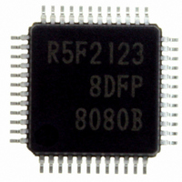
Manufacturer Part Number
R5F21238DFP#U0
Description
IC R8C/23 MCU FLASH 48-LQFP
Manufacturer
Renesas Electronics America
Series
R8C/2x/23r
Specifications of R5F21238DFP#U0
Core Size
16/32-Bit
Program Memory Size
64KB (64K x 8)
Peripherals
POR, Voltage Detect, WDT
Core Processor
R8C
Speed
20MHz
Connectivity
CAN, I²C, LIN, SIO, SSU, UART/USART
Number Of I /o
41
Program Memory Type
FLASH
Ram Size
3K x 8
Voltage - Supply (vcc/vdd)
2.7 V ~ 5.5 V
Data Converters
A/D 12x10b
Oscillator Type
Internal
Operating Temperature
-40°C ~ 85°C
Package / Case
48-LQFP
No. Of I/o's
41
Ram Memory Size
3KB
Cpu Speed
20MHz
No. Of Timers
4
Digital Ic Case Style
LQFP
Embedded Interface Type
CAN, I2C, UART
Rohs Compliant
Yes
Cpu Family
R8C
Device Core Size
16b
Frequency (max)
20MHz
Interface Type
I2C/UART
Total Internal Ram Size
3KB
# I/os (max)
41
Number Of Timers - General Purpose
5
Operating Supply Voltage (typ)
3.3/5V
Operating Supply Voltage (max)
5.5V
Operating Supply Voltage (min)
3V
On-chip Adc
12-chx10-bit
Instruction Set Architecture
CISC
Operating Temp Range
-40C to 85C
Operating Temperature Classification
Industrial
Mounting
Surface Mount
Pin Count
48
Package Type
LQFP
Lead Free Status / RoHS Status
Lead free / RoHS Compliant
For Use With
RCDK8C - KIT DEV EVAL FOR CAN R8C/23R0K521237S000BE - KIT DEV RSK R8C/23R0E521237CPE00 - EMULATOR COMPACT R8C/20/21/22/23
Eeprom Size
-
Lead Free Status / Rohs Status
Compliant
Available stocks
Company
Part Number
Manufacturer
Quantity
Price


21.
22.
20.4
20.5
20.6
20.7
22.1
22.2
22.3
22.4
22.5
22.6
22.7
22.8
22.9
22.10
20.3.2
20.4.1
20.4.2
20.4.3
20.4.4
20.4.5
20.5.1
20.6.1
20.7.1
22.1.1
22.1.2
22.1.3
22.1.4
22.2.1
22.2.2
22.2.3
22.2.4
22.2.5
22.3.1
22.3.2
22.3.3
22.3.4
22.5.1
22.5.2
22.7.1
22.7.2
22.7.3
22.9.1
22.10.1 Inserting a Bypass Capacitor between VCC and VSS Pins as a Countermeasure against Noise and
22.10.2 Countermeasures against Noise Error of Port Control Registers ..................................................... 494
Electrical Characteristics ............................................................................................................ 447
Usage Notes ............................................................................................................................... 467
CPU Rewrite Mode ............................................................................................................................... 421
Standard Serial I/O Mode ...................................................................................................................... 439
Parallel I/O Mode .................................................................................................................................. 443
Notes on Flash Memory ........................................................................................................................ 444
Notes on Clock Generation Circuit ....................................................................................................... 467
Notes on Interrupts ................................................................................................................................ 468
Notes on Timers .................................................................................................................................... 471
Notes on Serial Interface ....................................................................................................................... 483
Clock Synchronous Serial Interface ...................................................................................................... 484
Notes on Hardware LIN ........................................................................................................................ 485
Notes on CAN Module .......................................................................................................................... 486
Notes on Flash Memory ........................................................................................................................ 491
Notes on A/D Converter ....................................................................................................................... 490
Notes on Noise ..................................................................................................................................... 494
ROM Code Protect Function ............................................................................................................ 420
EW0 Mode ........................................................................................................................................ 422
EW1 Mode ........................................................................................................................................ 422
Software Commands ......................................................................................................................... 431
Status Registers ................................................................................................................................. 436
Full Status Check .............................................................................................................................. 437
ID Code Check Function .................................................................................................................. 439
ROM Code Protect Function ............................................................................................................ 443
CPU Rewrite Mode ........................................................................................................................... 444
Stop Mode ......................................................................................................................................... 467
Wait Mode ........................................................................................................................................ 467
Oscillation Stop Detection Function ................................................................................................. 467
Oscillation Circuit Constants ............................................................................................................ 467
Reading Address 00000h .................................................................................................................. 468
SP Setting .......................................................................................................................................... 468
External Interrupt and Key Input Interrupt ....................................................................................... 468
Changing Interrupt Sources .............................................................................................................. 469
Changing Interrupt Control Register Contents ................................................................................. 470
Notes on Timer RA ........................................................................................................................... 471
Notes on Timer RB ........................................................................................................................... 472
Notes on Timer RD ........................................................................................................................... 476
Notes on Timer RE ........................................................................................................................... 482
Notes on Clock Synchronous Serial I/O with Chip Select ............................................................... 484
Notes on I
Reading C0STR Register .................................................................................................................. 486
Performing CAN Configuration ....................................................................................................... 488
Suggestions to Reduce Power Consumption .................................................................................... 489
CPU Rewrite Mode ........................................................................................................................... 491
Latch-up ............................................................................................................................................ 494
2
C Bus Interface ............................................................................................................... 484
A - 6
Related parts for R5F21238DFP#U0
Image
Part Number
Description
Manufacturer
Datasheet
Request
R

Part Number:
Description:
KIT STARTER FOR M16C/29
Manufacturer:
Renesas Electronics America
Datasheet:

Part Number:
Description:
KIT STARTER FOR R8C/2D
Manufacturer:
Renesas Electronics America
Datasheet:

Part Number:
Description:
R0K33062P STARTER KIT
Manufacturer:
Renesas Electronics America
Datasheet:

Part Number:
Description:
KIT STARTER FOR R8C/23 E8A
Manufacturer:
Renesas Electronics America
Datasheet:

Part Number:
Description:
KIT STARTER FOR R8C/25
Manufacturer:
Renesas Electronics America
Datasheet:

Part Number:
Description:
KIT STARTER H8S2456 SHARPE DSPLY
Manufacturer:
Renesas Electronics America
Datasheet:

Part Number:
Description:
KIT STARTER FOR R8C38C
Manufacturer:
Renesas Electronics America
Datasheet:

Part Number:
Description:
KIT STARTER FOR R8C35C
Manufacturer:
Renesas Electronics America
Datasheet:

Part Number:
Description:
KIT STARTER FOR R8CL3AC+LCD APPS
Manufacturer:
Renesas Electronics America
Datasheet:
Part Number:
Description:
KIT STARTER FOR RX610
Manufacturer:
Renesas Electronics America
Datasheet:

Part Number:
Description:
KIT STARTER FOR R32C/118
Manufacturer:
Renesas Electronics America
Datasheet:

Part Number:
Description:
KIT DEV RSK-R8C/26-29
Manufacturer:
Renesas Electronics America
Datasheet:

Part Number:
Description:
KIT STARTER FOR SH7124
Manufacturer:
Renesas Electronics America
Datasheet:

Part Number:
Description:
KIT STARTER FOR H8SX/1622
Manufacturer:
Renesas Electronics America
Datasheet:

Part Number:
Description:
KIT DEV FOR SH7203
Manufacturer:
Renesas Electronics America
Datasheet: