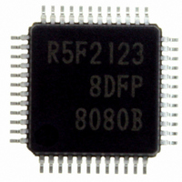
R5F21238DFP#U0 Renesas Electronics America, R5F21238DFP#U0 Datasheet - Page 423

R5F21238DFP#U0
Manufacturer Part Number
R5F21238DFP#U0
Description
IC R8C/23 MCU FLASH 48-LQFP
Manufacturer
Renesas Electronics America
Series
R8C/2x/23r
Specifications of R5F21238DFP#U0
Core Size
16/32-Bit
Program Memory Size
64KB (64K x 8)
Peripherals
POR, Voltage Detect, WDT
Core Processor
R8C
Speed
20MHz
Connectivity
CAN, I²C, LIN, SIO, SSU, UART/USART
Number Of I /o
41
Program Memory Type
FLASH
Ram Size
3K x 8
Voltage - Supply (vcc/vdd)
2.7 V ~ 5.5 V
Data Converters
A/D 12x10b
Oscillator Type
Internal
Operating Temperature
-40°C ~ 85°C
Package / Case
48-LQFP
No. Of I/o's
41
Ram Memory Size
3KB
Cpu Speed
20MHz
No. Of Timers
4
Digital Ic Case Style
LQFP
Embedded Interface Type
CAN, I2C, UART
Rohs Compliant
Yes
Cpu Family
R8C
Device Core Size
16b
Frequency (max)
20MHz
Interface Type
I2C/UART
Total Internal Ram Size
3KB
# I/os (max)
41
Number Of Timers - General Purpose
5
Operating Supply Voltage (typ)
3.3/5V
Operating Supply Voltage (max)
5.5V
Operating Supply Voltage (min)
3V
On-chip Adc
12-chx10-bit
Instruction Set Architecture
CISC
Operating Temp Range
-40C to 85C
Operating Temperature Classification
Industrial
Mounting
Surface Mount
Pin Count
48
Package Type
LQFP
Lead Free Status / RoHS Status
Lead free / RoHS Compliant
For Use With
RCDK8C - KIT DEV EVAL FOR CAN R8C/23R0K521237S000BE - KIT DEV RSK R8C/23R0E521237CPE00 - EMULATOR COMPACT R8C/20/21/22/23
Eeprom Size
-
Lead Free Status / Rohs Status
Compliant
Available stocks
Company
Part Number
Manufacturer
Quantity
Price
- Current page: 423 of 551
- Download datasheet (6Mb)
R8C/22 Group, R8C/23 Group
Rev.2.00 Aug 20, 2008
REJ09B0251-0200
Figure 19.2
A/D Control Register 0
b7 b6 b5 b4 b3 b2 b1 b0
NOTES:
1.
2.
3.
4.
If the ADCON0 register is rew ritten during A/D conversion, the conversion result is indeterminate.
When changing A/D operation mode, set the analog input pin again.
Set øAD frequency to 10 MHz or below .
The analog input pin can be select according to a combination of the CH0 to CH2 bits and the ADGSEL0 bit.
CH2 to CH0
000b
001b
010b
011b
100b
101b
110b
111b
ADCON0 Register
ADGSEL0 = 0
Bit Symbol
ADGSEL0
ADCON0
ADCAP
Symbol
(1)
ADST
CKS0
Page 401 of 501
CH0
CH1
CH2
AN0
AN1
AN2
AN3
AN4
AN5
AN6
AN7
MD
Analog input pin select bit
A/D operation mode select
bit
A/D input group select bit
A/D conversion automatic
start bit
A/D conversion start flag
Frequency select bit 0
(2)
ADGSEL0 = 1
Do not set
Address
Bit Name
00D6h
AN10
AN11
AN8
AN9
(4)
Refer to (4)
0 : On-shot mode
1 : Repeat mode
0 : Selects port P0 group (AN0 to AN7)
1 : Selects port P1 group (AN8 to AN11)
0 : Starts in softw are trigger (ADST bit)
1 : Starts in timer RD
0 : Disables A/D conversion
1 : Starts A/D conversion
[When CKS1 in ADCON1 register = 0]
0 : Select f4
1 : Select f2
[When CKS1 in ADCON1 register = 1]
0 : Select f1
1 : Select fOCO-F
(complementary PWM mode)
(3)
After Reset
Function
00h
19. A/D Converter
RW
RW
RW
RW
RW
RW
RW
RW
RW
Related parts for R5F21238DFP#U0
Image
Part Number
Description
Manufacturer
Datasheet
Request
R

Part Number:
Description:
KIT STARTER FOR M16C/29
Manufacturer:
Renesas Electronics America
Datasheet:

Part Number:
Description:
KIT STARTER FOR R8C/2D
Manufacturer:
Renesas Electronics America
Datasheet:

Part Number:
Description:
R0K33062P STARTER KIT
Manufacturer:
Renesas Electronics America
Datasheet:

Part Number:
Description:
KIT STARTER FOR R8C/23 E8A
Manufacturer:
Renesas Electronics America
Datasheet:

Part Number:
Description:
KIT STARTER FOR R8C/25
Manufacturer:
Renesas Electronics America
Datasheet:

Part Number:
Description:
KIT STARTER H8S2456 SHARPE DSPLY
Manufacturer:
Renesas Electronics America
Datasheet:

Part Number:
Description:
KIT STARTER FOR R8C38C
Manufacturer:
Renesas Electronics America
Datasheet:

Part Number:
Description:
KIT STARTER FOR R8C35C
Manufacturer:
Renesas Electronics America
Datasheet:

Part Number:
Description:
KIT STARTER FOR R8CL3AC+LCD APPS
Manufacturer:
Renesas Electronics America
Datasheet:

Part Number:
Description:
KIT STARTER FOR RX610
Manufacturer:
Renesas Electronics America
Datasheet:

Part Number:
Description:
KIT STARTER FOR R32C/118
Manufacturer:
Renesas Electronics America
Datasheet:

Part Number:
Description:
KIT DEV RSK-R8C/26-29
Manufacturer:
Renesas Electronics America
Datasheet:

Part Number:
Description:
KIT STARTER FOR SH7124
Manufacturer:
Renesas Electronics America
Datasheet:

Part Number:
Description:
KIT STARTER FOR H8SX/1622
Manufacturer:
Renesas Electronics America
Datasheet:

Part Number:
Description:
KIT DEV FOR SH7203
Manufacturer:
Renesas Electronics America
Datasheet:


