R8A77850ANBGV Renesas Electronics America, R8A77850ANBGV Datasheet - Page 534
R8A77850ANBGV
Manufacturer Part Number
R8A77850ANBGV
Description
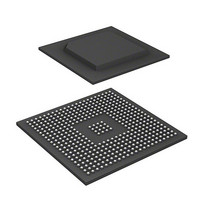
IC SUPERH MPU ROMLESS 436-BGA
Manufacturer
Renesas Electronics America
Series
SuperH® SH7780r
Datasheet
1.R8A77850AADBGV.pdf
(1694 pages)
Specifications of R8A77850ANBGV
Core Processor
SH-4A
Core Size
32-Bit
Speed
600MHz
Connectivity
Audio Codec, MMC, Serial Sound, SCI, SIO, SPI, SSI
Peripherals
DMA, POR, WDT
Number Of I /o
108
Program Memory Type
ROMless
Ram Size
8K x 8
Voltage - Supply (vcc/vdd)
1 V ~ 1.2 V
Oscillator Type
External
Operating Temperature
-20°C ~ 75°C
Package / Case
436-BGA
Lead Free Status / RoHS Status
Lead free / RoHS Compliant
Eeprom Size
-
Program Memory Size
-
Data Converters
-
Available stocks
Company
Part Number
Manufacturer
Quantity
Price
Company:

Part Number:
R8A77850ANBGV
Manufacturer:
Renesas Electronics America
Quantity:
10 000


12. DDR2-SDRAM Interface (DBSC2)
12.4.10 SDRAM Refresh Control Register 2 (DBRFCNT2)
The SDRAM refresh control register 2 (DBRFCNT2) is a readable/writable register. It is
initialized only upon power-on reset.
Rev.1.00 Jan. 10, 2008 Page 502 of 1658
REJ09B0261-0100
Initial value:
Initial value:
Bit
31
30 to 16 LV1TH14 to
R/W:
R/W:
BIt:
BIt:
Bit Name
⎯
LV1TH0
31
15
⎯
⎯
R
R
0
0
TH14
R/W
LV1
30
14
⎯
R
0
0
TH13
R/W
LV1
29
13
⎯
Initial
Value
0
001 0000
0000 0000
R
0
0
TH12
R/W
LV1
28
12
⎯
R
1
0
TH11
R/W
LV1
27
11
⎯
R
0
0
R/W
R
R/W
TH10
R/W
LV1
26
10
⎯
R
0
0
Description
Reserved
This bit is always read as 0. The write value should
always be 0.
Operation when a value other than 0 is written is not
guaranteed.
Level 1 Threshold Setting Bits
These bits set the threshold cycles for executing auto-
refresh when there is a vacancy in access requests
received via the SuperHyway bus.
The number of cycles is the number of DDR clock
cycles.
When the internal refresh counter value exceeds
LV1TH, and there are consecutive requests received via
the SuperHyway bus, request processing is given
priority over auto-refresh.
The relation between LV1TH and LV0TH must satisfy
the relation LV1TH ≥ LV0TH. Correct operation cannot
be guaranteed if LV1TH <LV0TH.
The value of LV1TH should be set larger than the
constraint TRAS between PRE and ACT set in the
SDRAM timing register 0. If a value equal to or less than
TRAS is set, Correct operation cannot be guaranteed.
R/W
TH9
LV1
25
⎯
R
0
9
0
R/W
TH8
LV1
24
⎯
R
0
8
0
R/W
R/W
TH7
TH7
LV1
LV0
23
0
7
1
R/W
R/W
TH6
TH6
LV1
LV0
22
0
6
0
R/W
R/W
TH5
TH5
LV1
LV0
21
0
5
0
R/W
R/W
LV1
TH4
LV0
TH4
20
0
4
0
R/W
R/W
LV1
TH3
LV0
TH3
19
0
3
0
R/W
R/W
TH2
TH2
LV1
LV0
18
0
2
0
R/W
R/W
TH1
TH1
LV1
LV0
17
0
1
0
R/W
R/W
TH0
TH0
LV1
LV0
16
0
0
0
Related parts for R8A77850ANBGV
Image
Part Number
Description
Manufacturer
Datasheet
Request
R

Part Number:
Description:
KIT STARTER FOR M16C/29
Manufacturer:
Renesas Electronics America
Datasheet:

Part Number:
Description:
KIT STARTER FOR R8C/2D
Manufacturer:
Renesas Electronics America
Datasheet:

Part Number:
Description:
R0K33062P STARTER KIT
Manufacturer:
Renesas Electronics America
Datasheet:

Part Number:
Description:
KIT STARTER FOR R8C/23 E8A
Manufacturer:
Renesas Electronics America
Datasheet:

Part Number:
Description:
KIT STARTER FOR R8C/25
Manufacturer:
Renesas Electronics America
Datasheet:

Part Number:
Description:
KIT STARTER H8S2456 SHARPE DSPLY
Manufacturer:
Renesas Electronics America
Datasheet:

Part Number:
Description:
KIT STARTER FOR R8C38C
Manufacturer:
Renesas Electronics America
Datasheet:

Part Number:
Description:
KIT STARTER FOR R8C35C
Manufacturer:
Renesas Electronics America
Datasheet:

Part Number:
Description:
KIT STARTER FOR R8CL3AC+LCD APPS
Manufacturer:
Renesas Electronics America
Datasheet:
Part Number:
Description:
KIT STARTER FOR RX610
Manufacturer:
Renesas Electronics America
Datasheet:

Part Number:
Description:
KIT STARTER FOR R32C/118
Manufacturer:
Renesas Electronics America
Datasheet:

Part Number:
Description:
KIT DEV RSK-R8C/26-29
Manufacturer:
Renesas Electronics America
Datasheet:

Part Number:
Description:
KIT STARTER FOR SH7124
Manufacturer:
Renesas Electronics America
Datasheet:

Part Number:
Description:
KIT STARTER FOR H8SX/1622
Manufacturer:
Renesas Electronics America
Datasheet:

Part Number:
Description:
KIT DEV FOR SH7203
Manufacturer:
Renesas Electronics America
Datasheet: