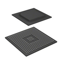
R8A77850ANBGV Renesas Electronics America, R8A77850ANBGV Datasheet - Page 181

R8A77850ANBGV
Manufacturer Part Number
R8A77850ANBGV
Description
IC SUPERH MPU ROMLESS 436-BGA
Manufacturer
Renesas Electronics America
Series
SuperH® SH7780r
Datasheet
1.R8A77850AADBGV.pdf
(1694 pages)
Specifications of R8A77850ANBGV
Core Processor
SH-4A
Core Size
32-Bit
Speed
600MHz
Connectivity
Audio Codec, MMC, Serial Sound, SCI, SIO, SPI, SSI
Peripherals
DMA, POR, WDT
Number Of I /o
108
Program Memory Type
ROMless
Ram Size
8K x 8
Voltage - Supply (vcc/vdd)
1 V ~ 1.2 V
Oscillator Type
External
Operating Temperature
-20°C ~ 75°C
Package / Case
436-BGA
Lead Free Status / RoHS Status
Lead free / RoHS Compliant
Eeprom Size
-
Program Memory Size
-
Data Converters
-
Available stocks
Company
Part Number
Manufacturer
Quantity
Price
Company:
Part Number:
R8A77850ANBGV
Manufacturer:
Renesas Electronics America
Quantity:
10 000
- Current page: 181 of 1694
- Download datasheet (9Mb)
7. Memory Management Unit (MMU)
The area from H'E000 0000 to H'E3FF FFFF comprises addresses for accessing the store queues
(SQs). In user mode, the access right is specified by the SQMD bit in MMUCR. For details, see
section 8.7, Store Queues.
The area from H'E500 0000 to H'E5FF FFFF comprises addresses for accessing the on-chip
memory. In user mode, the access right is specified by the RMD bit in RAMCR. For details, see
section 9, On-Chip Memory.
The area from H'F000 0000 to H'F0FF FFFF is used for direct access to the instruction cache
address array. For details, see section 8.6.1, IC Address Array.
The area from H'F100 0000 to H'F1FF FFFF is used for direct access to the instruction cache data
array. For details, see section 8.6.2, IC Data Array.
The area from H'F200 0000 to H'F2FF FFFF is used for direct access to the instruction TLB
address array. For details, see section 7.7.1, ITLB Address Array.
The area from H'F300 0000 to H'F37F FFFF is used for direct access to instruction TLB data
array. For details, see section 7.7.2, ITLB Data Array (TLB Compatible Mode) and section 7.7.3,
ITLB Data Array (TLB Extended Mode).
The area from H'F400 0000 to H'F4FF FFFF is used for direct access to the operand cache address
array. For details, see section 8.6.3, OC Address Array.
The area from H'F500 0000 to H'F5FF FFFF is used for direct access to the operand cache data
array. For details, see section 8.6.4, OC Data Array.
The area from H'F600 0000 to H'F60F FFFF is used for direct access to the unified TLB address
array. For details, see section 7.7.4, UTLB Address Array.
The area from H'F610 0000 to H'F61F FFFF is used for direct access to the PMB address array.
For details, see section 7.8.5, Memory-Mapped PMB Configuration.
The area from H'F700 0000 to H'F70F FFFF is used for direct access to unified TLB data array.
For details, see section 7.7.5, UTLB Data Array (TLB Compatible Mode) and 7.7.6, UTLB Data
Array (TLB Extended Mode).
The area from H'F710 0000 to H'F71F FFFF is used for direct access to the PMB data array. For
details, see section 7.8.5, Memory-Mapped PMB Configuration.
The area from H'FC00 0000 to H'FFFF FFFF is the on-chip peripheral module control register
area. For details, see register descriptions in each section of the hardware manual of the product.
Rev.1.00 Jan. 10, 2008 Page 149 of 1658
REJ09B0261-0100
Related parts for R8A77850ANBGV
Image
Part Number
Description
Manufacturer
Datasheet
Request
R

Part Number:
Description:
KIT STARTER FOR M16C/29
Manufacturer:
Renesas Electronics America
Datasheet:

Part Number:
Description:
KIT STARTER FOR R8C/2D
Manufacturer:
Renesas Electronics America
Datasheet:

Part Number:
Description:
R0K33062P STARTER KIT
Manufacturer:
Renesas Electronics America
Datasheet:

Part Number:
Description:
KIT STARTER FOR R8C/23 E8A
Manufacturer:
Renesas Electronics America
Datasheet:

Part Number:
Description:
KIT STARTER FOR R8C/25
Manufacturer:
Renesas Electronics America
Datasheet:

Part Number:
Description:
KIT STARTER H8S2456 SHARPE DSPLY
Manufacturer:
Renesas Electronics America
Datasheet:

Part Number:
Description:
KIT STARTER FOR R8C38C
Manufacturer:
Renesas Electronics America
Datasheet:

Part Number:
Description:
KIT STARTER FOR R8C35C
Manufacturer:
Renesas Electronics America
Datasheet:

Part Number:
Description:
KIT STARTER FOR R8CL3AC+LCD APPS
Manufacturer:
Renesas Electronics America
Datasheet:

Part Number:
Description:
KIT STARTER FOR RX610
Manufacturer:
Renesas Electronics America
Datasheet:

Part Number:
Description:
KIT STARTER FOR R32C/118
Manufacturer:
Renesas Electronics America
Datasheet:

Part Number:
Description:
KIT DEV RSK-R8C/26-29
Manufacturer:
Renesas Electronics America
Datasheet:

Part Number:
Description:
KIT STARTER FOR SH7124
Manufacturer:
Renesas Electronics America
Datasheet:

Part Number:
Description:
KIT STARTER FOR H8SX/1622
Manufacturer:
Renesas Electronics America
Datasheet:

Part Number:
Description:
KIT DEV FOR SH7203
Manufacturer:
Renesas Electronics America
Datasheet:


