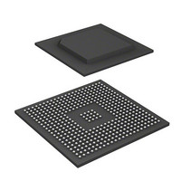
R8A77850ANBGV Renesas Electronics America, R8A77850ANBGV Datasheet - Page 383

R8A77850ANBGV
Manufacturer Part Number
R8A77850ANBGV
Description
IC SUPERH MPU ROMLESS 436-BGA
Manufacturer
Renesas Electronics America
Series
SuperH® SH7780r
Datasheet
1.R8A77850AADBGV.pdf
(1694 pages)
Specifications of R8A77850ANBGV
Core Processor
SH-4A
Core Size
32-Bit
Speed
600MHz
Connectivity
Audio Codec, MMC, Serial Sound, SCI, SIO, SPI, SSI
Peripherals
DMA, POR, WDT
Number Of I /o
108
Program Memory Type
ROMless
Ram Size
8K x 8
Voltage - Supply (vcc/vdd)
1 V ~ 1.2 V
Oscillator Type
External
Operating Temperature
-20°C ~ 75°C
Package / Case
436-BGA
Lead Free Status / RoHS Status
Lead free / RoHS Compliant
Eeprom Size
-
Program Memory Size
-
Data Converters
-
Available stocks
Company
Part Number
Manufacturer
Quantity
Price
Company:
Part Number:
R8A77850ANBGV
Manufacturer:
Renesas Electronics America
Quantity:
10 000
- Current page: 383 of 1694
- Download datasheet (9Mb)
Pin Name
WE0/REG
WE1
WE2/IORD
WE3/IOWR
WE4
WE5
WE6
WE7
RDY
IOIS16
BREQ
Function
Data Enable 0
Data Enable 1
Data Enable 2
Data Enable 3
Data Enable 4
Data Enable 5
Data Enable 6
Data Enable 7
Ready
16-Bit I/O
Bus Release
Request
I/O
O
O
O
O
O
O
O
O
I
I
I
input/output).
16-bit I/O designation signal in PCMCIA
Bus release request signal
Description
Write strobe signal for D7 to D0 in SRAM
interface setting
REG signal in PCMCIA interface setting
Write strobe signal for D15 to D8 in SRAM
interface setting
Write strobe signal in PCMCIA interface setting
Write strobe signal for D23 to D16 in SRAM
interface setting
IORD signal in PCMCIA interface setting
Write strobe signal for D31 to D24 in SRAM
IOWR signal in PCMCIA interface setting
Write strobe signal for D39 to D32 in SRAM
interface setting
Multiplexed with PCI/Port R0 (GPIO
Write strobe signal for D47 to D40 in SRAM
interface setting
Multiplexed with PCI/Port R1 (GPIO
input/output).
Write strobe signal for D55 to D48 in SRAM
interface setting
Multiplexed with PCI/Port R2 (GPIO
input/output).
Write strobe signal for D63 to D56 in SRAM
interface setting
Multiplexed with PCI/Port R3 (GPIO
input/output).
Wait cycle request signal
interface setting
Valid only in little endian mode
Multiplexed with MODE13, TCLK (TMU
input/output), and Port J0 (GPIO input/output)
Multiplexed with Port M1 (GPIO input/output).
interface setting
Rev.1.00 Jan. 10, 2008 Page 351 of 1658
11. Local Bus State Controller (LBSC)
REJ09B0261-0100
Related parts for R8A77850ANBGV
Image
Part Number
Description
Manufacturer
Datasheet
Request
R

Part Number:
Description:
KIT STARTER FOR M16C/29
Manufacturer:
Renesas Electronics America
Datasheet:

Part Number:
Description:
KIT STARTER FOR R8C/2D
Manufacturer:
Renesas Electronics America
Datasheet:

Part Number:
Description:
R0K33062P STARTER KIT
Manufacturer:
Renesas Electronics America
Datasheet:

Part Number:
Description:
KIT STARTER FOR R8C/23 E8A
Manufacturer:
Renesas Electronics America
Datasheet:

Part Number:
Description:
KIT STARTER FOR R8C/25
Manufacturer:
Renesas Electronics America
Datasheet:

Part Number:
Description:
KIT STARTER H8S2456 SHARPE DSPLY
Manufacturer:
Renesas Electronics America
Datasheet:

Part Number:
Description:
KIT STARTER FOR R8C38C
Manufacturer:
Renesas Electronics America
Datasheet:

Part Number:
Description:
KIT STARTER FOR R8C35C
Manufacturer:
Renesas Electronics America
Datasheet:

Part Number:
Description:
KIT STARTER FOR R8CL3AC+LCD APPS
Manufacturer:
Renesas Electronics America
Datasheet:

Part Number:
Description:
KIT STARTER FOR RX610
Manufacturer:
Renesas Electronics America
Datasheet:

Part Number:
Description:
KIT STARTER FOR R32C/118
Manufacturer:
Renesas Electronics America
Datasheet:

Part Number:
Description:
KIT DEV RSK-R8C/26-29
Manufacturer:
Renesas Electronics America
Datasheet:

Part Number:
Description:
KIT STARTER FOR SH7124
Manufacturer:
Renesas Electronics America
Datasheet:

Part Number:
Description:
KIT STARTER FOR H8SX/1622
Manufacturer:
Renesas Electronics America
Datasheet:

Part Number:
Description:
KIT DEV FOR SH7203
Manufacturer:
Renesas Electronics America
Datasheet:


