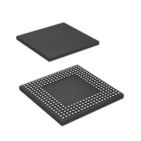
HD6417712BPV Renesas Electronics America, HD6417712BPV Datasheet - Page 86

HD6417712BPV
Manufacturer Part Number
HD6417712BPV
Description
MPU 1.5/3.3V 0K PB-FREE 256-BGA
Manufacturer
Renesas Electronics America
Series
SuperH® SH Ethernetr
Datasheet
1.HD6417712BPV.pdf
(980 pages)
Specifications of HD6417712BPV
Core Processor
SH-3 DSP
Core Size
32-Bit
Speed
200MHz
Connectivity
EBI/EMI, Ethernet, FIFO, SCI, SIO
Peripherals
DMA, POR, WDT
Number Of I /o
24
Program Memory Type
ROMless
Ram Size
16K x 8
Voltage - Supply (vcc/vdd)
1.4 V ~ 1.6 V
Oscillator Type
External
Operating Temperature
-20°C ~ 75°C
Package / Case
256-BGA
Lead Free Status / RoHS Status
Lead free / RoHS Compliant
Eeprom Size
-
Program Memory Size
-
Data Converters
-
Available stocks
Company
Part Number
Manufacturer
Quantity
Price
Company:
Part Number:
HD6417712BPV
Manufacturer:
Renesas Electronics America
Quantity:
10 000
- Current page: 86 of 980
- Download datasheet (6Mb)
Section 2 CPU
2.4
2.4.1
Register operands are always longwords (32 bits). When the memory operand is only a byte (8
bits) or a word (16 bits), it is sign-extended into a longword when loaded into a register.
2.4.2
Memory data formats are classified into byte, word, and longword. Memory can be accessed in
byte, word, and longword. When the memory operand is only a byte (8 bits) or a word (16 bits), it
is sign-extended into a longword when loaded into a register.
An address error will occur if word data starting from an address other than 2n or longword data
starting from an address other than 4n is accessed. In such cases, the data accessed cannot be
guaranteed.
When a word or longword operand is accessed, the byte positions on the memory corresponding to
the word or longword data on the register is determined to the specified endian mode (big endian
or little endian).
Figure 2.7 shows a byte correspondence in big endian mode. In big endian mode, the MSB byte in
the register corresponds to the lowest address in the memory, and the LSB the in the register
corresponds to the highest address. For example, if the contents of the general register R0 is stored
at an address indicated by the general register R1 in longword, the MSB byte of the R0 is stored at
the address indicated by the R1 and the LSB byte of the R1 register is stored at the address
indicated by the (R1 +3).
The on-chip device registers assigned to memory are accessed in big endian mode. Note that the
available access size (byte, word, or long word) differs in each register.
Note: The CPU instruction codes of this LSI must be stored in word units. In big endian mode,
Rev. 1.00 Dec. 27, 2005 Page 42 of 932
REJ09B0269-0100
the instruction code must be stored from upper byte to lower byte in this order from the
word boundary of the memory.
Data Formats
Register Data Format
Memory Data Formats
31
Longword
0
Related parts for HD6417712BPV
Image
Part Number
Description
Manufacturer
Datasheet
Request
R

Part Number:
Description:
KIT STARTER FOR M16C/29
Manufacturer:
Renesas Electronics America
Datasheet:

Part Number:
Description:
KIT STARTER FOR R8C/2D
Manufacturer:
Renesas Electronics America
Datasheet:

Part Number:
Description:
R0K33062P STARTER KIT
Manufacturer:
Renesas Electronics America
Datasheet:

Part Number:
Description:
KIT STARTER FOR R8C/23 E8A
Manufacturer:
Renesas Electronics America
Datasheet:

Part Number:
Description:
KIT STARTER FOR R8C/25
Manufacturer:
Renesas Electronics America
Datasheet:

Part Number:
Description:
KIT STARTER H8S2456 SHARPE DSPLY
Manufacturer:
Renesas Electronics America
Datasheet:

Part Number:
Description:
KIT STARTER FOR R8C38C
Manufacturer:
Renesas Electronics America
Datasheet:

Part Number:
Description:
KIT STARTER FOR R8C35C
Manufacturer:
Renesas Electronics America
Datasheet:

Part Number:
Description:
KIT STARTER FOR R8CL3AC+LCD APPS
Manufacturer:
Renesas Electronics America
Datasheet:

Part Number:
Description:
KIT STARTER FOR RX610
Manufacturer:
Renesas Electronics America
Datasheet:

Part Number:
Description:
KIT STARTER FOR R32C/118
Manufacturer:
Renesas Electronics America
Datasheet:

Part Number:
Description:
KIT DEV RSK-R8C/26-29
Manufacturer:
Renesas Electronics America
Datasheet:

Part Number:
Description:
KIT STARTER FOR SH7124
Manufacturer:
Renesas Electronics America
Datasheet:

Part Number:
Description:
KIT STARTER FOR H8SX/1622
Manufacturer:
Renesas Electronics America
Datasheet:

Part Number:
Description:
KIT DEV FOR SH7203
Manufacturer:
Renesas Electronics America
Datasheet:


