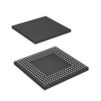
HD6417712BPV Renesas Electronics America, HD6417712BPV Datasheet - Page 80

HD6417712BPV
Manufacturer Part Number
HD6417712BPV
Description
MPU 1.5/3.3V 0K PB-FREE 256-BGA
Manufacturer
Renesas Electronics America
Series
SuperH® SH Ethernetr
Datasheet
1.HD6417712BPV.pdf
(980 pages)
Specifications of HD6417712BPV
Core Processor
SH-3 DSP
Core Size
32-Bit
Speed
200MHz
Connectivity
EBI/EMI, Ethernet, FIFO, SCI, SIO
Peripherals
DMA, POR, WDT
Number Of I /o
24
Program Memory Type
ROMless
Ram Size
16K x 8
Voltage - Supply (vcc/vdd)
1.4 V ~ 1.6 V
Oscillator Type
External
Operating Temperature
-20°C ~ 75°C
Package / Case
256-BGA
Lead Free Status / RoHS Status
Lead free / RoHS Compliant
Eeprom Size
-
Program Memory Size
-
Data Converters
-
Available stocks
Company
Part Number
Manufacturer
Quantity
Price
Company:
Part Number:
HD6417712BPV
Manufacturer:
Renesas Electronics America
Quantity:
10 000
- Current page: 80 of 980
- Download datasheet (6Mb)
Section 2 CPU
2.3.2
The system registers: multiply and accumulate registers (MACH/MACL) and procedure register
(PR) as system registers can be accessed by the LDS and STS instructions.
Multiply and Accumulate Registers (MACH/MACL): The multiply and accumulate registers
(MACH/MACL) store the results of multiplication and accumulation instructions or multiplication
instructions. The MACH/MACL registers also store addition values for the multiplication and
accumulations. After reset, these registers are undefined. The MACH and MACL registers store
upper 32 bits and lower 32 bits, respectively.
Procedure Register (PR): The procedure register (PR) stores the return address for a subroutine
call using the BSR, BSRF, or JSR instruction. The return address stored in the PR register is
restored to the program counter (PC) by the RTS (return from the subroutine) instruction. After
reset, this register is undefined.
Rev. 1.00 Dec. 27, 2005 Page 36 of 932
REJ09B0269-0100
System Registers
31
R0
R1
R2
R3
R4
R5
R6
R7
R8
R9
R10
R11
R12
R13
R14
R15
*1,*2
*2
*2
*2
*2
*2
*2
*2
Figure 2.4 General Registers
0
General Registers: Undefined after reset
Notes: *1 R0 functions as an index register in the indexed
*2 R0–R7 are banked registers. In user mode,
BANK0 is used. In privileged mode, either
R0_BANK0 to R7_BANK0 or R0_BANK1 to
R7_BANK1 is selected by the RB bit of the SR
register.
register-indirect addressing mode and indexed
GBR-indirect addressing mode. In some
instructions, only R0 can be used as the source
or destination register.
Related parts for HD6417712BPV
Image
Part Number
Description
Manufacturer
Datasheet
Request
R

Part Number:
Description:
KIT STARTER FOR M16C/29
Manufacturer:
Renesas Electronics America
Datasheet:

Part Number:
Description:
KIT STARTER FOR R8C/2D
Manufacturer:
Renesas Electronics America
Datasheet:

Part Number:
Description:
R0K33062P STARTER KIT
Manufacturer:
Renesas Electronics America
Datasheet:

Part Number:
Description:
KIT STARTER FOR R8C/23 E8A
Manufacturer:
Renesas Electronics America
Datasheet:

Part Number:
Description:
KIT STARTER FOR R8C/25
Manufacturer:
Renesas Electronics America
Datasheet:

Part Number:
Description:
KIT STARTER H8S2456 SHARPE DSPLY
Manufacturer:
Renesas Electronics America
Datasheet:

Part Number:
Description:
KIT STARTER FOR R8C38C
Manufacturer:
Renesas Electronics America
Datasheet:

Part Number:
Description:
KIT STARTER FOR R8C35C
Manufacturer:
Renesas Electronics America
Datasheet:

Part Number:
Description:
KIT STARTER FOR R8CL3AC+LCD APPS
Manufacturer:
Renesas Electronics America
Datasheet:

Part Number:
Description:
KIT STARTER FOR RX610
Manufacturer:
Renesas Electronics America
Datasheet:

Part Number:
Description:
KIT STARTER FOR R32C/118
Manufacturer:
Renesas Electronics America
Datasheet:

Part Number:
Description:
KIT DEV RSK-R8C/26-29
Manufacturer:
Renesas Electronics America
Datasheet:

Part Number:
Description:
KIT STARTER FOR SH7124
Manufacturer:
Renesas Electronics America
Datasheet:

Part Number:
Description:
KIT STARTER FOR H8SX/1622
Manufacturer:
Renesas Electronics America
Datasheet:

Part Number:
Description:
KIT DEV FOR SH7203
Manufacturer:
Renesas Electronics America
Datasheet:


