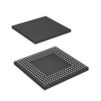
HD6417712BPV Renesas Electronics America, HD6417712BPV Datasheet - Page 498

HD6417712BPV
Manufacturer Part Number
HD6417712BPV
Description
MPU 1.5/3.3V 0K PB-FREE 256-BGA
Manufacturer
Renesas Electronics America
Series
SuperH® SH Ethernetr
Datasheet
1.HD6417712BPV.pdf
(980 pages)
Specifications of HD6417712BPV
Core Processor
SH-3 DSP
Core Size
32-Bit
Speed
200MHz
Connectivity
EBI/EMI, Ethernet, FIFO, SCI, SIO
Peripherals
DMA, POR, WDT
Number Of I /o
24
Program Memory Type
ROMless
Ram Size
16K x 8
Voltage - Supply (vcc/vdd)
1.4 V ~ 1.6 V
Oscillator Type
External
Operating Temperature
-20°C ~ 75°C
Package / Case
256-BGA
Lead Free Status / RoHS Status
Lead free / RoHS Compliant
Eeprom Size
-
Program Memory Size
-
Data Converters
-
Available stocks
Company
Part Number
Manufacturer
Quantity
Price
Company:
Part Number:
HD6417712BPV
Manufacturer:
Renesas Electronics America
Quantity:
10 000
- Current page: 498 of 980
- Download datasheet (6Mb)
Section 12 Bus State Controller (BSC)
12.5.10 Wait between Access Cycles
As the operating frequency of LSIs becomes higher, the off-operation of the data buffer often
collides with the next data access when the read operation from devices with slow access speed is
completed. As a result of these collisions, the reliability of the device is low and malfunctions may
occur. This LSI has a function that avoids data collisions by inserting wait cycles between
continuous access cycles.
The number of wait cycles between access cycles can be set by bits IWW[2:0], IWRWD[2:0],
IWRWS[2:0], IWRRD[2:0], and IWRRS[2:0] in CSnBCR, and bits DMAIW[2:0] and DMAIWA
in CMNCR. The conditions for setting the wait cycles between access cycles (idle cycles) are
shown below.
1. Continuous accesses are write-read or write-write
2. Continuous accesses are read-write for different spaces
3. Continuous accesses are read-write for the same space
4. Continuous accesses are read-read for different spaces
5. Continuous accesses are read-read for the same space
6. Data output from an external device caused by DMA single transfer is followed by data output
7. Data output from an external device caused by DMA single transfer is followed by any type of
12.5.11 Bus Arbitration
To prevent device malfunction while the bus mastership is transferred between master and slave,
the LSI negates all of the bus control signals before bus release. When the bus mastership is
received, all of the bus control signals are first negated and then driven appropriately. In this case,
output buffer contention can be prevented because the master and slave drive the same signals
with the same values. In addition, to prevent noise while the bus control signal is in the high
impedance state, pull-up resistors must be connected to these control signals.
Bus mastership is transferred at the boundary of bus cycles. Namely, bus mastership is released
immediately after receiving a bus request when a bus cycle is not being performed. The release of
bus mastership is delayed until the bus cycle is complete when a bus cycle is in progress. Even
when from outside the LSI it looks like a bus cycle is not being performed, a bus cycle may be
performing internally, started by inserting wait cycles between access cycles. Therefore, it cannot
be immediately determined whether or not bus mastership has been released by looking at the CSn
Rev. 1.00 Dec. 27, 2005 Page 454 of 932
REJ09B0269-0100
from another device that includes this LSI (DMAIWA = 0)
access (DMAIWA = 1)
Related parts for HD6417712BPV
Image
Part Number
Description
Manufacturer
Datasheet
Request
R

Part Number:
Description:
KIT STARTER FOR M16C/29
Manufacturer:
Renesas Electronics America
Datasheet:

Part Number:
Description:
KIT STARTER FOR R8C/2D
Manufacturer:
Renesas Electronics America
Datasheet:

Part Number:
Description:
R0K33062P STARTER KIT
Manufacturer:
Renesas Electronics America
Datasheet:

Part Number:
Description:
KIT STARTER FOR R8C/23 E8A
Manufacturer:
Renesas Electronics America
Datasheet:

Part Number:
Description:
KIT STARTER FOR R8C/25
Manufacturer:
Renesas Electronics America
Datasheet:

Part Number:
Description:
KIT STARTER H8S2456 SHARPE DSPLY
Manufacturer:
Renesas Electronics America
Datasheet:

Part Number:
Description:
KIT STARTER FOR R8C38C
Manufacturer:
Renesas Electronics America
Datasheet:

Part Number:
Description:
KIT STARTER FOR R8C35C
Manufacturer:
Renesas Electronics America
Datasheet:

Part Number:
Description:
KIT STARTER FOR R8CL3AC+LCD APPS
Manufacturer:
Renesas Electronics America
Datasheet:

Part Number:
Description:
KIT STARTER FOR RX610
Manufacturer:
Renesas Electronics America
Datasheet:

Part Number:
Description:
KIT STARTER FOR R32C/118
Manufacturer:
Renesas Electronics America
Datasheet:

Part Number:
Description:
KIT DEV RSK-R8C/26-29
Manufacturer:
Renesas Electronics America
Datasheet:

Part Number:
Description:
KIT STARTER FOR SH7124
Manufacturer:
Renesas Electronics America
Datasheet:

Part Number:
Description:
KIT STARTER FOR H8SX/1622
Manufacturer:
Renesas Electronics America
Datasheet:

Part Number:
Description:
KIT DEV FOR SH7203
Manufacturer:
Renesas Electronics America
Datasheet:


