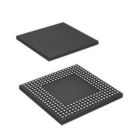
HD6417712BPV Renesas Electronics America, HD6417712BPV Datasheet - Page 466

HD6417712BPV
Manufacturer Part Number
HD6417712BPV
Description
MPU 1.5/3.3V 0K PB-FREE 256-BGA
Manufacturer
Renesas Electronics America
Series
SuperH® SH Ethernetr
Datasheet
1.HD6417712BPV.pdf
(980 pages)
Specifications of HD6417712BPV
Core Processor
SH-3 DSP
Core Size
32-Bit
Speed
200MHz
Connectivity
EBI/EMI, Ethernet, FIFO, SCI, SIO
Peripherals
DMA, POR, WDT
Number Of I /o
24
Program Memory Type
ROMless
Ram Size
16K x 8
Voltage - Supply (vcc/vdd)
1.4 V ~ 1.6 V
Oscillator Type
External
Operating Temperature
-20°C ~ 75°C
Package / Case
256-BGA
Lead Free Status / RoHS Status
Lead free / RoHS Compliant
Eeprom Size
-
Program Memory Size
-
Data Converters
-
Available stocks
Company
Part Number
Manufacturer
Quantity
Price
Company:
Part Number:
HD6417712BPV
Manufacturer:
Renesas Electronics America
Quantity:
10 000
- Current page: 466 of 980
- Download datasheet (6Mb)
Section 12 Bus State Controller (BSC)
then when precharging is completed, the access is performed by issuing an ACTV command
followed by a READ or WRIT command. If this is followed by an access to a different row
address, the access time will be longer because of the precharging performed after the access
request is issued. The number of cycles between issuance of the PRE command and the ACTV
command is determined by the TRP[1:0] bits in CSnWCR.
In a write, when an auto-precharge is performed, a command cannot be issued to the same bank
for a period of Trwl + Tap cycles after issuance of the WRITA command. When bank active mode
is used, READ or WRIT commands can be issued successively if the row address is the same. The
number of cycles can thus be reduced by Trwl + Tap cycles for each write.
There is a limit on tRAS, the time for placing each bank in the active state. If there is no guarantee
that there will not be a cache hit and another row address will be accessed within the period in
which this value is maintained by program execution, it is necessary to set auto-refresh and set the
refresh cycle to no more than the maximum value of tRAS.
A burst read cycle without auto-precharge is shown in figure 12.19, a burst read cycle for the same
row address in figure 12.20, and a burst read cycle for different row addresses in figure 12.21.
Similarly, a single write cycle without auto-precharge is shown in figure 12.22, a single write
cycle for the same row address in figure 12.23, and a single write cycle for different row addresses
in figure 12.24.
In figure 12.20, a Tnop cycle in which no operation is performed is inserted before the Tc cycle
that issues the READ command. The Tnop cycle is inserted to acquire two cycles of CAS latency
for the DQMxx signal that specifies the read byte in the data read from the SDRAM. If the CAS
latency is specified as two cycles or more, the Tnop cycle is not inserted because the two cycles of
latency can be acquired even if the DQMxx signal is asserted after the Tc cycle.
When bank active mode is set, if only accesses to the respective banks in the area 3 space are
considered, as long as accesses to the same row address continue, the operation starts with the
cycle in figure 12.19 or 12.22, followed by repetition of the cycle in figure 12.20 or 12.23. An
access to a different area during this time has no effect. If there is an access to a different row
address in the bank active state, after this is detected the bus cycle in figure 12.21 or 12.24 is
executed instead of that in figure 12.20 or 12.23. In bank active mode, too, all banks become
inactive after a refresh cycle or after the bus is released as the result of bus arbitration.
Rev. 1.00 Dec. 27, 2005 Page 422 of 932
REJ09B0269-0100
Related parts for HD6417712BPV
Image
Part Number
Description
Manufacturer
Datasheet
Request
R

Part Number:
Description:
KIT STARTER FOR M16C/29
Manufacturer:
Renesas Electronics America
Datasheet:

Part Number:
Description:
KIT STARTER FOR R8C/2D
Manufacturer:
Renesas Electronics America
Datasheet:

Part Number:
Description:
R0K33062P STARTER KIT
Manufacturer:
Renesas Electronics America
Datasheet:

Part Number:
Description:
KIT STARTER FOR R8C/23 E8A
Manufacturer:
Renesas Electronics America
Datasheet:

Part Number:
Description:
KIT STARTER FOR R8C/25
Manufacturer:
Renesas Electronics America
Datasheet:

Part Number:
Description:
KIT STARTER H8S2456 SHARPE DSPLY
Manufacturer:
Renesas Electronics America
Datasheet:

Part Number:
Description:
KIT STARTER FOR R8C38C
Manufacturer:
Renesas Electronics America
Datasheet:

Part Number:
Description:
KIT STARTER FOR R8C35C
Manufacturer:
Renesas Electronics America
Datasheet:

Part Number:
Description:
KIT STARTER FOR R8CL3AC+LCD APPS
Manufacturer:
Renesas Electronics America
Datasheet:

Part Number:
Description:
KIT STARTER FOR RX610
Manufacturer:
Renesas Electronics America
Datasheet:

Part Number:
Description:
KIT STARTER FOR R32C/118
Manufacturer:
Renesas Electronics America
Datasheet:

Part Number:
Description:
KIT DEV RSK-R8C/26-29
Manufacturer:
Renesas Electronics America
Datasheet:

Part Number:
Description:
KIT STARTER FOR SH7124
Manufacturer:
Renesas Electronics America
Datasheet:

Part Number:
Description:
KIT STARTER FOR H8SX/1622
Manufacturer:
Renesas Electronics America
Datasheet:

Part Number:
Description:
KIT DEV FOR SH7203
Manufacturer:
Renesas Electronics America
Datasheet:


