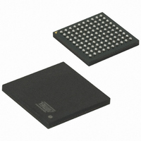
ATSAM3U4CA-CU Atmel, ATSAM3U4CA-CU Datasheet - Page 954

ATSAM3U4CA-CU
Manufacturer Part Number
ATSAM3U4CA-CU
Description
IC MCU 32BIT 256KB FLSH 100TFBGA
Manufacturer
Atmel
Series
SAM3Ur
Specifications of ATSAM3U4CA-CU
Core Processor
ARM® Cortex-M3™
Core Size
32-Bit
Speed
96MHz
Connectivity
EBI/EMI, I²C, MMC, SPI, SSC, UART/USART, USB
Peripherals
Brown-out Detect/Reset, DMA, I²S, POR, PWM, WDT
Number Of I /o
57
Program Memory Size
256KB (256K x 8)
Program Memory Type
FLASH
Ram Size
52K x 8
Voltage - Supply (vcc/vdd)
1.65 V ~ 1.95 V
Data Converters
A/D 4x10b, 4x12b
Oscillator Type
Internal
Operating Temperature
-40°C ~ 85°C
Package / Case
100-TFBGA
Processor Series
ATSAM3x
Core
ARM Cortex M3
Data Bus Width
32 bit
Data Ram Size
52 KB
Interface Type
3xUSART, TWI, 4xSPI, Bus
Maximum Clock Frequency
96 MHz
Number Of Programmable I/os
57
Number Of Timers
8
Operating Supply Voltage
1.62 V to 3.6 V
Maximum Operating Temperature
+ 85 C
Mounting Style
SMD/SMT
3rd Party Development Tools
JTRACE-CM3, MDK-ARM, RL-ARM, ULINK2
Development Tools By Supplier
ATSAM3U-EK
Minimum Operating Temperature
- 40 C
Lead Free Status / RoHS Status
Lead free / RoHS Compliant
Eeprom Size
-
Lead Free Status / Rohs Status
Lead free / RoHS Compliant
Available stocks
Company
Part Number
Manufacturer
Quantity
Price
Part Number:
ATSAM3U4CA-CU
Manufacturer:
ATMEL/爱特梅尔
Quantity:
20 000
- Current page: 954 of 1171
- Download datasheet (25Mb)
39.6.8.5
954
954
SAM3U Series
SAM3U Series
Bulk IN or Interrupt IN: Sending a Packet Under Application Control (Device to Host)
The application can write one or several banks.
A simple algorithm can be used by the application to send packets regardless of the number of
banks associated to the endpoint.
Algorithm Description for Each Packet:
The application is notified that it is possible to write a new packet to the DPR by the
TX_PK_RDY interrupt. This interrupt can be enabled or masked by setting the TX_PK_RDY bit
in the UDPHS_EPTCTLENB/UDPHS_EPTCTLDIS register.
Algorithm Description to Fill Several Packets:
Using the previous algorithm, the application is interrupted for each packet. It is possible to
reduce the application overhead by writing linearly several banks at the same time. The
AUTO_VALID bit in the UDPHS_EPTCTLx must be set by writing the AUTO_VALID bit in the
UDPHS_EPTCTLENBx register.
The auto-valid-bank mechanism allows the transfer of data (IN and OUT) without the interven-
tion of the CPU. This means that bank validation (set TX_PK_RDY or clear the RX_BK_RDY bit)
is done by hardware.
The application is notified that all banks are free, so that it is possible to write another burst of
packets by the BUSY_BANK interrupt. This interrupt can be enabled or masked by setting the
BUSY_BANK flag in the UDPHS_EPTCTLENB and UDPHS_EPTCTLDIS registers.
This algorithm must not be used for isochronous transfer. In this case, the ping-pong mechanism
does not operate.
A Z e r o L e n g t h P a c k e t c a n b e s e n t b y s e t t i n g j u s t t h e T X _ P K T R D Y f l a g i n t h e
UDPHS_EPTSETSTAx register.
• The application waits for TX_PK_RDY flag to be cleared in the UDPHS_EPTSTAx register
• The application writes one USB packet of data in the DPR through the
• The application sets TX_PK_RDY flag in the UDPHS_EPTSETSTAx register.
• The application checks the BUSY_BANK_STA field in the UDPHS_EPTSTAx register. The
• The application writes a number of bytes inferior to the number of free DPR banks for the
• If the last packet is incomplete (i.e., the last byte of the bank has not been written) the
before it can perform a write access to the DPR.
memory window.
application must wait that at least one bank is free.
endpoint. Each time the application writes the last byte of a bank, the TX_PK_RDY signal is
automatically set by the UDPHS.
application must set the TX_PK_RDY bit in the UDPHS_EPTSETSTAx register.
64
KB endpoint logical
6430D–ATARM–25-Mar-11
6430D–ATARM–25-Mar-11
Related parts for ATSAM3U4CA-CU
Image
Part Number
Description
Manufacturer
Datasheet
Request
R

Part Number:
Description:
KIT EVAL FOR AT91SAM3U CORTEX
Manufacturer:
Atmel
Datasheet:

Part Number:
Description:
AT91 ARM Thumb-based Microcontrollers
Manufacturer:
ATMEL [ATMEL Corporation]
Datasheet:

Part Number:
Description:
DEV KIT FOR AVR/AVR32
Manufacturer:
Atmel
Datasheet:

Part Number:
Description:
INTERVAL AND WIPE/WASH WIPER CONTROL IC WITH DELAY
Manufacturer:
ATMEL Corporation
Datasheet:

Part Number:
Description:
Low-Voltage Voice-Switched IC for Hands-Free Operation
Manufacturer:
ATMEL Corporation
Datasheet:

Part Number:
Description:
MONOLITHIC INTEGRATED FEATUREPHONE CIRCUIT
Manufacturer:
ATMEL Corporation
Datasheet:

Part Number:
Description:
AM-FM Receiver IC U4255BM-M
Manufacturer:
ATMEL Corporation
Datasheet:

Part Number:
Description:
Monolithic Integrated Feature Phone Circuit
Manufacturer:
ATMEL Corporation
Datasheet:

Part Number:
Description:
Multistandard Video-IF and Quasi Parallel Sound Processing
Manufacturer:
ATMEL Corporation
Datasheet:

Part Number:
Description:
High-performance EE PLD
Manufacturer:
ATMEL Corporation
Datasheet:

Part Number:
Description:
8-bit Flash Microcontroller
Manufacturer:
ATMEL Corporation
Datasheet:

Part Number:
Description:
2-Wire Serial EEPROM
Manufacturer:
ATMEL Corporation
Datasheet:


