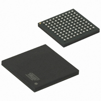
ATSAM3U4CA-CU Atmel, ATSAM3U4CA-CU Datasheet - Page 206

ATSAM3U4CA-CU
Manufacturer Part Number
ATSAM3U4CA-CU
Description
IC MCU 32BIT 256KB FLSH 100TFBGA
Manufacturer
Atmel
Series
SAM3Ur
Specifications of ATSAM3U4CA-CU
Core Processor
ARM® Cortex-M3™
Core Size
32-Bit
Speed
96MHz
Connectivity
EBI/EMI, I²C, MMC, SPI, SSC, UART/USART, USB
Peripherals
Brown-out Detect/Reset, DMA, I²S, POR, PWM, WDT
Number Of I /o
57
Program Memory Size
256KB (256K x 8)
Program Memory Type
FLASH
Ram Size
52K x 8
Voltage - Supply (vcc/vdd)
1.65 V ~ 1.95 V
Data Converters
A/D 4x10b, 4x12b
Oscillator Type
Internal
Operating Temperature
-40°C ~ 85°C
Package / Case
100-TFBGA
Processor Series
ATSAM3x
Core
ARM Cortex M3
Data Bus Width
32 bit
Data Ram Size
52 KB
Interface Type
3xUSART, TWI, 4xSPI, Bus
Maximum Clock Frequency
96 MHz
Number Of Programmable I/os
57
Number Of Timers
8
Operating Supply Voltage
1.62 V to 3.6 V
Maximum Operating Temperature
+ 85 C
Mounting Style
SMD/SMT
3rd Party Development Tools
JTRACE-CM3, MDK-ARM, RL-ARM, ULINK2
Development Tools By Supplier
ATSAM3U-EK
Minimum Operating Temperature
- 40 C
Lead Free Status / RoHS Status
Lead free / RoHS Compliant
Eeprom Size
-
Lead Free Status / Rohs Status
Lead free / RoHS Compliant
Available stocks
Company
Part Number
Manufacturer
Quantity
Price
Part Number:
ATSAM3U4CA-CU
Manufacturer:
ATMEL/爱特梅尔
Quantity:
20 000
- Current page: 206 of 1171
- Download datasheet (25Mb)
13.20.15 Auxiliary Fault Status Register
• IMPDEF
Implementation defined. The bits map to the AUXFAULT input signals.
Each AFSR bit maps directly to an AUXFAULT input of the processor, and a single-cycle HIGH signal on the input sets the
corresponding AFSR bit to one. It remains set to 1 until you write 1 to the bit to clear it to zero.
When an AFSR bit is latched as one, an exception does not occur. Use an interrupt if an exception is required.
13.20.16 System control block design hints and tips
206
31
23
15
7
SAM3U Series
30
22
14
6
The AFSR contains additional system fault information. See the register summary in
30 on page 180
This register is read, write to clear. This means that bits in the register read normally, but writing
1 to any bit clears that bit to 0.
The bit assignments are:
Ensure software uses aligned accesses of the correct size to access the system control block
registers:
The processor does not support unaligned accesses to system control block registers.
In a fault handler. to determine the true faulting address:
Software must follow this sequence because another higher priority exception might change the
MMFAR or BFAR value. For example, if a higher priority handler preempts the current fault han-
dler, the other fault might change the MMFAR or BFAR value.
• except for the CFSR and SHPR1-SHPR3, it must use aligned word accesses
• for the CFSR and SHPR1-SHPR3 it can use byte or aligned halfword or word accesses.
• Read and save the MMFAR or BFAR value.
• Read the MMARVALID bit in the MMFSR, or the BFARVALID bit in the BFSR. The MMFAR or
BFAR address is valid only if this bit is 1.
29
21
13
5
for its attributes.
28
20
12
4
IMPDEF
IMPDEF
IMPDEF
IMPDEF
27
19
11
3
26
18
10
2
25
17
9
1
6430D–ATARM–25-Mar-11
Table 13-
24
16
8
0
Related parts for ATSAM3U4CA-CU
Image
Part Number
Description
Manufacturer
Datasheet
Request
R

Part Number:
Description:
KIT EVAL FOR AT91SAM3U CORTEX
Manufacturer:
Atmel
Datasheet:

Part Number:
Description:
AT91 ARM Thumb-based Microcontrollers
Manufacturer:
ATMEL [ATMEL Corporation]
Datasheet:

Part Number:
Description:
DEV KIT FOR AVR/AVR32
Manufacturer:
Atmel
Datasheet:

Part Number:
Description:
INTERVAL AND WIPE/WASH WIPER CONTROL IC WITH DELAY
Manufacturer:
ATMEL Corporation
Datasheet:

Part Number:
Description:
Low-Voltage Voice-Switched IC for Hands-Free Operation
Manufacturer:
ATMEL Corporation
Datasheet:

Part Number:
Description:
MONOLITHIC INTEGRATED FEATUREPHONE CIRCUIT
Manufacturer:
ATMEL Corporation
Datasheet:

Part Number:
Description:
AM-FM Receiver IC U4255BM-M
Manufacturer:
ATMEL Corporation
Datasheet:

Part Number:
Description:
Monolithic Integrated Feature Phone Circuit
Manufacturer:
ATMEL Corporation
Datasheet:

Part Number:
Description:
Multistandard Video-IF and Quasi Parallel Sound Processing
Manufacturer:
ATMEL Corporation
Datasheet:

Part Number:
Description:
High-performance EE PLD
Manufacturer:
ATMEL Corporation
Datasheet:

Part Number:
Description:
8-bit Flash Microcontroller
Manufacturer:
ATMEL Corporation
Datasheet:

Part Number:
Description:
2-Wire Serial EEPROM
Manufacturer:
ATMEL Corporation
Datasheet:


