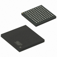
ATSAM3U4CA-CU Atmel, ATSAM3U4CA-CU Datasheet - Page 432

ATSAM3U4CA-CU
Manufacturer Part Number
ATSAM3U4CA-CU
Description
IC MCU 32BIT 256KB FLSH 100TFBGA
Manufacturer
Atmel
Series
SAM3Ur
Specifications of ATSAM3U4CA-CU
Core Processor
ARM® Cortex-M3™
Core Size
32-Bit
Speed
96MHz
Connectivity
EBI/EMI, I²C, MMC, SPI, SSC, UART/USART, USB
Peripherals
Brown-out Detect/Reset, DMA, I²S, POR, PWM, WDT
Number Of I /o
57
Program Memory Size
256KB (256K x 8)
Program Memory Type
FLASH
Ram Size
52K x 8
Voltage - Supply (vcc/vdd)
1.65 V ~ 1.95 V
Data Converters
A/D 4x10b, 4x12b
Oscillator Type
Internal
Operating Temperature
-40°C ~ 85°C
Package / Case
100-TFBGA
Processor Series
ATSAM3x
Core
ARM Cortex M3
Data Bus Width
32 bit
Data Ram Size
52 KB
Interface Type
3xUSART, TWI, 4xSPI, Bus
Maximum Clock Frequency
96 MHz
Number Of Programmable I/os
57
Number Of Timers
8
Operating Supply Voltage
1.62 V to 3.6 V
Maximum Operating Temperature
+ 85 C
Mounting Style
SMD/SMT
3rd Party Development Tools
JTRACE-CM3, MDK-ARM, RL-ARM, ULINK2
Development Tools By Supplier
ATSAM3U-EK
Minimum Operating Temperature
- 40 C
Lead Free Status / RoHS Status
Lead free / RoHS Compliant
Eeprom Size
-
Lead Free Status / Rohs Status
Lead free / RoHS Compliant
Available stocks
Company
Part Number
Manufacturer
Quantity
Price
Part Number:
ATSAM3U4CA-CU
Manufacturer:
ATMEL/爱特梅尔
Quantity:
20 000
- Current page: 432 of 1171
- Download datasheet (25Mb)
25.18.20 SMC Timings Register
Name:
Address:
Access:
Reset:
• TCLR: CLE to REN Low Delay
Command Latch Enable falling edge to Read Enable falling edge timing.
Latch Enable Falling to Read Enable Falling = (TCLR[3] * 64) + TCLR[2:0] clock cycles.
• TADL: ALE to Data Start
Last address latch cycle to the first rising edge of WEN for data input.
Last address latch to first rising edge of WEN = (TADL[3] * 64) + TADL[2:0] clock cycles.
• TAR: ALE to REN Low Delay
Address Latch Enable falling edge to Read Enable falling edge timing.
Address Latch Enable to Read Enable = (TAR[3] * 64) + TAR[2:0] clock cycles.
• OCMS: Off Chip Memory Scrambling Enable
When set to one, the memory scrambling is activated.
• TRR: Ready to REN Low Delay
Ready/Busy signal to Read Enable falling edge timing.
Read to REN = (TRR[3] * 64) + TRR[2:0] clock cycles.
• TWB: WEN High to REN to Busy
Write Enable rising edge to Ready/Busy falling edge timing.
Write Enable to Read/Busy = (TWB[3] * 64) + TWB[2:0] clock cycles.
• RBNSEL: Ready/Busy Line Selection
This field indicates the selected Ready/Busy Line from the RBN bundle.
• NFSEL: NAND Flash Selection
If this bit is set to one, the chip select is assigned to NAND Flash write enable and read enable lines drive the Error Correct-
ing Code module.
432
432
NFSEL
31
23
15
–
–
7
SAM3U Series
SAM3U Series
0x400E007C [0], 0x400E0090 [1], 0x400E00A4 [2], 0x400E00B8 [3]
SMC_TIMINGSx [x=0..3]
Read-write
0x00000000
30
22
14
–
–
6
TADL
RBNSEL
29
21
13
–
–
5
OCMS
28
20
12
–
4
27
19
11
3
26
18
10
2
TCLR
TWB
TRR
TAR
25
17
9
1
6430D–ATARM–25-Mar-11
6430D–ATARM–25-Mar-11
24
16
8
0
Related parts for ATSAM3U4CA-CU
Image
Part Number
Description
Manufacturer
Datasheet
Request
R

Part Number:
Description:
KIT EVAL FOR AT91SAM3U CORTEX
Manufacturer:
Atmel
Datasheet:

Part Number:
Description:
AT91 ARM Thumb-based Microcontrollers
Manufacturer:
ATMEL [ATMEL Corporation]
Datasheet:

Part Number:
Description:
DEV KIT FOR AVR/AVR32
Manufacturer:
Atmel
Datasheet:

Part Number:
Description:
INTERVAL AND WIPE/WASH WIPER CONTROL IC WITH DELAY
Manufacturer:
ATMEL Corporation
Datasheet:

Part Number:
Description:
Low-Voltage Voice-Switched IC for Hands-Free Operation
Manufacturer:
ATMEL Corporation
Datasheet:

Part Number:
Description:
MONOLITHIC INTEGRATED FEATUREPHONE CIRCUIT
Manufacturer:
ATMEL Corporation
Datasheet:

Part Number:
Description:
AM-FM Receiver IC U4255BM-M
Manufacturer:
ATMEL Corporation
Datasheet:

Part Number:
Description:
Monolithic Integrated Feature Phone Circuit
Manufacturer:
ATMEL Corporation
Datasheet:

Part Number:
Description:
Multistandard Video-IF and Quasi Parallel Sound Processing
Manufacturer:
ATMEL Corporation
Datasheet:

Part Number:
Description:
High-performance EE PLD
Manufacturer:
ATMEL Corporation
Datasheet:

Part Number:
Description:
8-bit Flash Microcontroller
Manufacturer:
ATMEL Corporation
Datasheet:

Part Number:
Description:
2-Wire Serial EEPROM
Manufacturer:
ATMEL Corporation
Datasheet:


