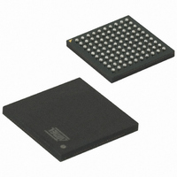
ATSAM3U4CA-CU Atmel, ATSAM3U4CA-CU Datasheet - Page 384

ATSAM3U4CA-CU
Manufacturer Part Number
ATSAM3U4CA-CU
Description
IC MCU 32BIT 256KB FLSH 100TFBGA
Manufacturer
Atmel
Series
SAM3Ur
Specifications of ATSAM3U4CA-CU
Core Processor
ARM® Cortex-M3™
Core Size
32-Bit
Speed
96MHz
Connectivity
EBI/EMI, I²C, MMC, SPI, SSC, UART/USART, USB
Peripherals
Brown-out Detect/Reset, DMA, I²S, POR, PWM, WDT
Number Of I /o
57
Program Memory Size
256KB (256K x 8)
Program Memory Type
FLASH
Ram Size
52K x 8
Voltage - Supply (vcc/vdd)
1.65 V ~ 1.95 V
Data Converters
A/D 4x10b, 4x12b
Oscillator Type
Internal
Operating Temperature
-40°C ~ 85°C
Package / Case
100-TFBGA
Processor Series
ATSAM3x
Core
ARM Cortex M3
Data Bus Width
32 bit
Data Ram Size
52 KB
Interface Type
3xUSART, TWI, 4xSPI, Bus
Maximum Clock Frequency
96 MHz
Number Of Programmable I/os
57
Number Of Timers
8
Operating Supply Voltage
1.62 V to 3.6 V
Maximum Operating Temperature
+ 85 C
Mounting Style
SMD/SMT
3rd Party Development Tools
JTRACE-CM3, MDK-ARM, RL-ARM, ULINK2
Development Tools By Supplier
ATSAM3U-EK
Minimum Operating Temperature
- 40 C
Lead Free Status / RoHS Status
Lead free / RoHS Compliant
Eeprom Size
-
Lead Free Status / Rohs Status
Lead free / RoHS Compliant
Available stocks
Company
Part Number
Manufacturer
Quantity
Price
Part Number:
ATSAM3U4CA-CU
Manufacturer:
ATMEL/爱特梅尔
Quantity:
20 000
- Current page: 384 of 1171
- Download datasheet (25Mb)
25.16 NAND Flash Controller Operations
25.16.1
25.16.2
Figure 25-31. NFC/NAND Flash Access Example
384
384
SAM3U Series
SAM3U Series
NFC Overview
NFC Control Registers
The NFC can handle automatic transfers, sending the commands and address to the NAND
Flash and transferring the contents of the page (for read and write) to the NFC SRAM. It mini-
mizes the CPU overhead.
NAND Flash Read and NAND Flash Program operations can be performed through the NFC
Command Registers. In order to minimize CPU intervention and latency, commands are posted
in a command buffer. This buffer provides zero wait state latency. The detailed description of the
command encoding scheme is explained below.
The NFC handles automatic transfer between the external NAND Flash and the chip via the
NFC SRAM. It is done via NFC Command Registers.
The NFC Command Registers are very efficient to use. When writing to these registers:
So, in one single access the command is sent and immediately executed by the NFC. Even two
commands can be programmed within a single access (CMD1, CMD2) depending on the
VCMD2 value.
The NFC can send up to 5 Address cycles.
Figure 25-31
ory and correspondence with NFC Address Command Register.
For more details refer to
The NFC Command Registers can be found at address
Table 25-4, “External Memory
Reading the NFC command register (to any address) will give the status of the NFC. Especially
useful to know if the NFC is busy, for example.
• the address of the register (NFCADDR_CMD) contains the command used,
• the data of the register (NFCDATA_ADDT) contains the address to be sent to the NAND
Flash.
00h
Col. Add1
below shows a typical NAND Flash Page Read Command of a NAND Flash Mem-
CMD1
Column Address
Col. Add2
“NFC Address Command” on page
Depends on ACYCLE value
ADD cycles (0 to 5)
Mapping”.)
Row Add1 Row Add2 Row Add3
Row Address
If VCMD2 = 1
CMD2
386.
0x68000000 - 0x6FFFFFFF.
30h
6430D–ATARM–25-Mar-11
6430D–ATARM–25-Mar-11
(See
Related parts for ATSAM3U4CA-CU
Image
Part Number
Description
Manufacturer
Datasheet
Request
R

Part Number:
Description:
KIT EVAL FOR AT91SAM3U CORTEX
Manufacturer:
Atmel
Datasheet:

Part Number:
Description:
AT91 ARM Thumb-based Microcontrollers
Manufacturer:
ATMEL [ATMEL Corporation]
Datasheet:

Part Number:
Description:
DEV KIT FOR AVR/AVR32
Manufacturer:
Atmel
Datasheet:

Part Number:
Description:
INTERVAL AND WIPE/WASH WIPER CONTROL IC WITH DELAY
Manufacturer:
ATMEL Corporation
Datasheet:

Part Number:
Description:
Low-Voltage Voice-Switched IC for Hands-Free Operation
Manufacturer:
ATMEL Corporation
Datasheet:

Part Number:
Description:
MONOLITHIC INTEGRATED FEATUREPHONE CIRCUIT
Manufacturer:
ATMEL Corporation
Datasheet:

Part Number:
Description:
AM-FM Receiver IC U4255BM-M
Manufacturer:
ATMEL Corporation
Datasheet:

Part Number:
Description:
Monolithic Integrated Feature Phone Circuit
Manufacturer:
ATMEL Corporation
Datasheet:

Part Number:
Description:
Multistandard Video-IF and Quasi Parallel Sound Processing
Manufacturer:
ATMEL Corporation
Datasheet:

Part Number:
Description:
High-performance EE PLD
Manufacturer:
ATMEL Corporation
Datasheet:

Part Number:
Description:
8-bit Flash Microcontroller
Manufacturer:
ATMEL Corporation
Datasheet:

Part Number:
Description:
2-Wire Serial EEPROM
Manufacturer:
ATMEL Corporation
Datasheet:


