DF38602RFT10 Renesas Electronics America, DF38602RFT10 Datasheet - Page 387
DF38602RFT10
Manufacturer Part Number
DF38602RFT10
Description
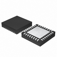
MCU 3V 16K 32-QFN
Manufacturer
Renesas Electronics America
Series
H8® H8/300H SLPr
Datasheet
1.DF38602RFT10.pdf
(554 pages)
Specifications of DF38602RFT10
Core Processor
H8/300H
Core Size
16-Bit
Speed
10MHz
Connectivity
I²C, IrDA, SCI, SSU
Peripherals
POR, PWM, WDT
Number Of I /o
13
Program Memory Size
16KB (16K x 8)
Program Memory Type
FLASH
Ram Size
1K x 8
Voltage - Supply (vcc/vdd)
2.7 V ~ 3.6 V
Data Converters
A/D 6x10b
Oscillator Type
Internal
Operating Temperature
-20°C ~ 75°C
Package / Case
32-QFN
Lead Free Status / RoHS Status
Contains lead / RoHS non-compliant
Eeprom Size
-
Other names
HD64F38602RFT10
HD64F38602RFT10
HD64F38602RFT10
Available stocks
Company
Part Number
Manufacturer
Quantity
Price
Company:

Part Number:
DF38602RFT10V
Manufacturer:
Renesas Electronics America
Quantity:
135


17.4
The A/D converter operates by successive approximation with 10-bit resolution. When changing
the conversion time or analog input channel, in order to prevent incorrect operation, first clear the
bit ADSF to 0 in ADSR.
17.4.1
1. A/D conversion is started from the selected channel when the ADSF bit in ADSR is set to 1,
2. When A/D conversion is completed, the result is transferred to the A/D result register.
3. On completion of conversion, the IRRAD flag in IRR2 is set to 1. If the IENAD bit in IENR2
4. The ADSF bit remains set to 1 during A/D conversion. When A/D conversion ends, the ADSF
17.4.2
The A/D converter can also start A/D conversion by input of an external trigger signal. External
trigger input is enabled at the ADTRG pin when the ADTSTCHG bit in PMRB is set to 1* and the
TRGE bit in AMR is set to 1. Then when the input signal edge designated in the ADTRGNEG bit
in IEGR is detected at the ADTRG pin, the ADSF bit in ADSR will be set to 1, starting A/D
conversion.
Figure 17.2 shows the timing.
Note: * The ADTRG input pin is shared with the TEST pin. Therefore when the pin is used as
according to software.
is set to 1 at this time, an A/D conversion end interrupt request is generated.
bit is automatically cleared to 0 and the A/D converter enters the wait state.
Operation
the ADTRG pin, reset should be cleared while the 0-fixed signal is input to the TEST
pin. Then the ADTSTCHG bit should be set to 1 after the TEST signal is fixed.
A/D Conversion
External Trigger Input Timing
ADTRG
(when
ADTRGNEG = 0)
φ
ADSF
Figure 17.2 External Trigger Input Timing
A/D conversion
Rev. 3.00 May 15, 2007 Page 353 of 518
Section 17 A/D Converter
REJ09B0152-0300
Related parts for DF38602RFT10
Image
Part Number
Description
Manufacturer
Datasheet
Request
R

Part Number:
Description:
KIT STARTER FOR M16C/29
Manufacturer:
Renesas Electronics America
Datasheet:

Part Number:
Description:
KIT STARTER FOR R8C/2D
Manufacturer:
Renesas Electronics America
Datasheet:

Part Number:
Description:
R0K33062P STARTER KIT
Manufacturer:
Renesas Electronics America
Datasheet:

Part Number:
Description:
KIT STARTER FOR R8C/23 E8A
Manufacturer:
Renesas Electronics America
Datasheet:

Part Number:
Description:
KIT STARTER FOR R8C/25
Manufacturer:
Renesas Electronics America
Datasheet:

Part Number:
Description:
KIT STARTER H8S2456 SHARPE DSPLY
Manufacturer:
Renesas Electronics America
Datasheet:

Part Number:
Description:
KIT STARTER FOR R8C38C
Manufacturer:
Renesas Electronics America
Datasheet:

Part Number:
Description:
KIT STARTER FOR R8C35C
Manufacturer:
Renesas Electronics America
Datasheet:

Part Number:
Description:
KIT STARTER FOR R8CL3AC+LCD APPS
Manufacturer:
Renesas Electronics America
Datasheet:
Part Number:
Description:
KIT STARTER FOR RX610
Manufacturer:
Renesas Electronics America
Datasheet:

Part Number:
Description:
KIT STARTER FOR R32C/118
Manufacturer:
Renesas Electronics America
Datasheet:

Part Number:
Description:
KIT DEV RSK-R8C/26-29
Manufacturer:
Renesas Electronics America
Datasheet:

Part Number:
Description:
KIT STARTER FOR SH7124
Manufacturer:
Renesas Electronics America
Datasheet:

Part Number:
Description:
KIT STARTER FOR H8SX/1622
Manufacturer:
Renesas Electronics America
Datasheet:

Part Number:
Description:
KIT DEV FOR SH7203
Manufacturer:
Renesas Electronics America
Datasheet: