DF38602RFT10 Renesas Electronics America, DF38602RFT10 Datasheet - Page 13
DF38602RFT10
Manufacturer Part Number
DF38602RFT10
Description
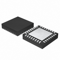
MCU 3V 16K 32-QFN
Manufacturer
Renesas Electronics America
Series
H8® H8/300H SLPr
Datasheet
1.DF38602RFT10.pdf
(554 pages)
Specifications of DF38602RFT10
Core Processor
H8/300H
Core Size
16-Bit
Speed
10MHz
Connectivity
I²C, IrDA, SCI, SSU
Peripherals
POR, PWM, WDT
Number Of I /o
13
Program Memory Size
16KB (16K x 8)
Program Memory Type
FLASH
Ram Size
1K x 8
Voltage - Supply (vcc/vdd)
2.7 V ~ 3.6 V
Data Converters
A/D 6x10b
Oscillator Type
Internal
Operating Temperature
-20°C ~ 75°C
Package / Case
32-QFN
Lead Free Status / RoHS Status
Contains lead / RoHS non-compliant
Eeprom Size
-
Other names
HD64F38602RFT10
HD64F38602RFT10
HD64F38602RFT10
Available stocks
Company
Part Number
Manufacturer
Quantity
Price
Company:

Part Number:
DF38602RFT10V
Manufacturer:
Renesas Electronics America
Quantity:
135


Section 5 Power-Down Modes ............................................................................77
5.1
5.2
5.3
5.4
5.5
5.6
Section 6 ROM ....................................................................................................99
6.1
6.2
4.5.2
4.5.3
4.5.4
4.5.5
4.5.6
4.5.7
Register Descriptions ........................................................................................................... 78
5.1.1
5.1.2
5.1.3
Mode Transitions and States of LSI..................................................................................... 83
5.2.1
5.2.2
5.2.3
5.2.4
5.2.5
5.2.6
Direct Transition .................................................................................................................. 91
5.3.1
5.3.2
5.3.3
5.3.4
5.3.5
5.3.6
5.3.7
Module Standby Function.................................................................................................... 96
On-Chip Oscillator and Operation Mode ............................................................................. 96
Usage Notes ......................................................................................................................... 97
5.6.1
5.6.2
Block Configuration........................................................................................................... 100
Register Descriptions ......................................................................................................... 101
6.2.1
6.2.2
Notes on Board Design ........................................................................................... 74
Definition of Oscillation Stabilization Wait Time .................................................. 74
Note on Subclock Stop State................................................................................... 76
Note on the Oscillation Stabilization of Resonators ............................................... 76
Note on Using Power-On Reset .............................................................................. 76
Note on Using On-Chip Emulator .......................................................................... 76
System Control Register 1 (SYSCR1) .................................................................... 78
System Control Register 2 (SYSCR2) .................................................................... 80
Clock Halt Registers 1 and 2 (CKSTPR1 and CKSTPR2) ..................................... 81
Sleep Mode ............................................................................................................. 87
Standby Mode ......................................................................................................... 88
Watch Mode............................................................................................................ 88
Subsleep Mode........................................................................................................ 89
Subactive Mode ...................................................................................................... 89
Active (Medium-Speed) Mode ............................................................................... 90
Direct Transition from Active (High-Speed)
Mode to Active (Medium-Speed) Mode ................................................................. 91
Direct Transition from Active (High-Speed) Mode to Subactive Mode................. 92
Direct Transition from Active (Medium-Speed)
Mode to Active (High-Speed) Mode ...................................................................... 92
Direct Transition from Active (Medium-Speed) Mode to Subactive Mode ........... 93
Direct Transition from Subactive Mode to Active (High-Speed) Mode................. 93
Direct Transition from Subactive Mode to Active (Medium-Speed) Mode ........... 94
Notes on External Input Signal Changes before/after Direct Transition................. 95
Standby Mode Transition and Pin States ................................................................ 97
Notes on External Input Signal Changes before/after Standby Mode..................... 97
Flash Memory Control Register 1 (FLMCR1)...................................................... 101
Flash Memory Control Register 2 (FLMCR2)...................................................... 102
Rev. 3.00 May 15, 2007 Page xi of xxxii
Related parts for DF38602RFT10
Image
Part Number
Description
Manufacturer
Datasheet
Request
R

Part Number:
Description:
KIT STARTER FOR M16C/29
Manufacturer:
Renesas Electronics America
Datasheet:

Part Number:
Description:
KIT STARTER FOR R8C/2D
Manufacturer:
Renesas Electronics America
Datasheet:

Part Number:
Description:
R0K33062P STARTER KIT
Manufacturer:
Renesas Electronics America
Datasheet:

Part Number:
Description:
KIT STARTER FOR R8C/23 E8A
Manufacturer:
Renesas Electronics America
Datasheet:

Part Number:
Description:
KIT STARTER FOR R8C/25
Manufacturer:
Renesas Electronics America
Datasheet:

Part Number:
Description:
KIT STARTER H8S2456 SHARPE DSPLY
Manufacturer:
Renesas Electronics America
Datasheet:

Part Number:
Description:
KIT STARTER FOR R8C38C
Manufacturer:
Renesas Electronics America
Datasheet:

Part Number:
Description:
KIT STARTER FOR R8C35C
Manufacturer:
Renesas Electronics America
Datasheet:

Part Number:
Description:
KIT STARTER FOR R8CL3AC+LCD APPS
Manufacturer:
Renesas Electronics America
Datasheet:
Part Number:
Description:
KIT STARTER FOR RX610
Manufacturer:
Renesas Electronics America
Datasheet:

Part Number:
Description:
KIT STARTER FOR R32C/118
Manufacturer:
Renesas Electronics America
Datasheet:

Part Number:
Description:
KIT DEV RSK-R8C/26-29
Manufacturer:
Renesas Electronics America
Datasheet:

Part Number:
Description:
KIT STARTER FOR SH7124
Manufacturer:
Renesas Electronics America
Datasheet:

Part Number:
Description:
KIT STARTER FOR H8SX/1622
Manufacturer:
Renesas Electronics America
Datasheet:

Part Number:
Description:
KIT DEV FOR SH7203
Manufacturer:
Renesas Electronics America
Datasheet: