DF38602RFT10 Renesas Electronics America, DF38602RFT10 Datasheet - Page 373
DF38602RFT10
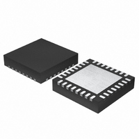
Manufacturer Part Number
DF38602RFT10
Description
MCU 3V 16K 32-QFN
Manufacturer
Renesas Electronics America
Series
H8® H8/300H SLPr
Datasheet
1.DF38602RFT10.pdf
(554 pages)
Specifications of DF38602RFT10
Core Processor
H8/300H
Core Size
16-Bit
Speed
10MHz
Connectivity
I²C, IrDA, SCI, SSU
Peripherals
POR, PWM, WDT
Number Of I /o
13
Program Memory Size
16KB (16K x 8)
Program Memory Type
FLASH
Ram Size
1K x 8
Voltage - Supply (vcc/vdd)
2.7 V ~ 3.6 V
Data Converters
A/D 6x10b
Oscillator Type
Internal
Operating Temperature
-20°C ~ 75°C
Package / Case
32-QFN
Lead Free Status / RoHS Status
Contains lead / RoHS non-compliant
Eeprom Size
-
Other names
HD64F38602RFT10
HD64F38602RFT10
HD64F38602RFT10
Available stocks
Company
Part Number
Manufacturer
Quantity
Price
Company:

Part Number:
DF38602RFT10V
Manufacturer:
Renesas Electronics America
Quantity:
135


(3)
In receive mode, data is latched at the rise of the transfer clock. The transfer clock is output when
MST in ICCR1 is 1, and is input when MST is 0. For receive mode operation timing, refer to
figure 16.15. The reception procedure and operations in receive mode are described below.
1. Set the ICE bit in ICCR1 to 1. Set the MST and CKS3 to CKS0 bits in ICCR1 to 1. (Initial
2. When the transfer clock is output, set MST to 1 to start outputting the receive clock.
3. When the receive operation is completed, data is transferred from ICDRS to ICDRR and
4. To stop receiving when MST = 1, set RCVD in ICCR1 to 1, then read ICDRR. Then, SCL is
processing
ICDRS
ICDRR
RDRF
(Input)
MST
TRS
SCL
SDA
User
setting)
RDRF in ICSR is set. When MST = 1, the next byte can be received, so the clock is
continually output. The continuous reception is performed by reading ICDRR every time
RDRF is set. When the 8th clock is risen while RDRF is 1, the overrun is detected and
AL/OVE in ICSR is set. At this time, the previous reception data is retained in ICDRR.
fixed high after receiving the next byte data.
Receive Operation
[2] Set MST
(when outputting the clock)
Bit 0
1
Figure 16.15 Receive Mode Operation Timing
Data 1
Bit 1
2
Bit 6
7
[3] Read ICDRR
Bit 7
8
Bit 0
Data 2
1
Data 1
Rev. 3.00 May 15, 2007 Page 339 of 516
Section 16 I
Bit 6
7
Bit 7
2
C Bus Interface 2 (IIC2)
8
REJ09B0152-0300
Bit 0
1
[3] Read ICDRR
Data 2
Data 3
Bit 1
2
Related parts for DF38602RFT10
Image
Part Number
Description
Manufacturer
Datasheet
Request
R

Part Number:
Description:
KIT STARTER FOR M16C/29
Manufacturer:
Renesas Electronics America
Datasheet:

Part Number:
Description:
KIT STARTER FOR R8C/2D
Manufacturer:
Renesas Electronics America
Datasheet:

Part Number:
Description:
R0K33062P STARTER KIT
Manufacturer:
Renesas Electronics America
Datasheet:

Part Number:
Description:
KIT STARTER FOR R8C/23 E8A
Manufacturer:
Renesas Electronics America
Datasheet:

Part Number:
Description:
KIT STARTER FOR R8C/25
Manufacturer:
Renesas Electronics America
Datasheet:

Part Number:
Description:
KIT STARTER H8S2456 SHARPE DSPLY
Manufacturer:
Renesas Electronics America
Datasheet:

Part Number:
Description:
KIT STARTER FOR R8C38C
Manufacturer:
Renesas Electronics America
Datasheet:

Part Number:
Description:
KIT STARTER FOR R8C35C
Manufacturer:
Renesas Electronics America
Datasheet:

Part Number:
Description:
KIT STARTER FOR R8CL3AC+LCD APPS
Manufacturer:
Renesas Electronics America
Datasheet:
Part Number:
Description:
KIT STARTER FOR RX610
Manufacturer:
Renesas Electronics America
Datasheet:

Part Number:
Description:
KIT STARTER FOR R32C/118
Manufacturer:
Renesas Electronics America
Datasheet:

Part Number:
Description:
KIT DEV RSK-R8C/26-29
Manufacturer:
Renesas Electronics America
Datasheet:

Part Number:
Description:
KIT STARTER FOR SH7124
Manufacturer:
Renesas Electronics America
Datasheet:

Part Number:
Description:
KIT STARTER FOR H8SX/1622
Manufacturer:
Renesas Electronics America
Datasheet:

Part Number:
Description:
KIT DEV FOR SH7203
Manufacturer:
Renesas Electronics America
Datasheet: