DF38602RFT10 Renesas Electronics America, DF38602RFT10 Datasheet - Page 327
DF38602RFT10
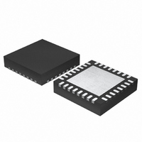
Manufacturer Part Number
DF38602RFT10
Description
MCU 3V 16K 32-QFN
Manufacturer
Renesas Electronics America
Series
H8® H8/300H SLPr
Datasheet
1.DF38602RFT10.pdf
(554 pages)
Specifications of DF38602RFT10
Core Processor
H8/300H
Core Size
16-Bit
Speed
10MHz
Connectivity
I²C, IrDA, SCI, SSU
Peripherals
POR, PWM, WDT
Number Of I /o
13
Program Memory Size
16KB (16K x 8)
Program Memory Type
FLASH
Ram Size
1K x 8
Voltage - Supply (vcc/vdd)
2.7 V ~ 3.6 V
Data Converters
A/D 6x10b
Oscillator Type
Internal
Operating Temperature
-20°C ~ 75°C
Package / Case
32-QFN
Lead Free Status / RoHS Status
Contains lead / RoHS non-compliant
Eeprom Size
-
Other names
HD64F38602RFT10
HD64F38602RFT10
HD64F38602RFT10
Available stocks
Company
Part Number
Manufacturer
Quantity
Price
Company:

Part Number:
DF38602RFT10V
Manufacturer:
Renesas Electronics America
Quantity:
135


15.3.6
SSRDR is an 8-bit register that stores received serial data. When the SSU has received one byte of
serial data, it transfers the received serial data from SSTRSR and the data is stored. After this,
SSTRSR is receive-enabled. As SSTRSR and SSRDR function as a double buffer in this way,
continuous receive operations are possible. SSRDR is a read-only register and cannot be written to
by the CPU. SSRDR is initialized to H'00.
15.3.7
SSTDR is an 8-bit register that stores serial data for transmission. SSTDR can be read or written
to by the CPU at all times. When the SSU detects that SSTRSR is empty, it transfers the transmit
data written in SSTDR to SSTRSR and starts serial transmission. If the next transmit data has
already been written to SSTDR during serial transmission, continuous serial transmission is
possible. SSTDR is initialized to H'00.
15.3.8
SSTRSR is a shift register that transmits and receives serial data. When transmit data is transferred
from SSTDR to SSTRSR, bit 0 in SSTDR is transferred to bit 0 in SSTRSR while the MLS bit in
SSMR is 0 (LSB-first transfer) and bit 7 in SSTDR is transferred to bit 0 in SSTRSR while the
MLS bit in SSMR is 1 (MSB-first transfer). SSTRSR cannot be directly accessed by the CPU.
15.4
15.4.1
Transfer clock can be selected from eight internal clocks and an external clock. When this module
is used, the SSCK pin must be selected as a serial clock by setting the SCKS bit in SSCRH to 1.
When the MSS bit in SSCRH is 1, an internal clock is selected and the SSCK pin is in the output
state. If transfer is started, the SSCK pin outputs clocks of the transfer rate set in the CKS2 to
CKS0 bits in SSMR. When the MSS bit is 0, an external clock is selected and the SSCK pin is in
the input state.
SS Receive Data Register (SSRDR)
SS Transmit Data Register (SSTDR)
SS Shift Register (SSTRSR)
Operation
Transfer Clock
Section 15 Synchronous Serial Communication Unit (SSU)
Rev. 3.00 May 15, 2007 Page 293 of 518
REJ09B0152-0300
Related parts for DF38602RFT10
Image
Part Number
Description
Manufacturer
Datasheet
Request
R

Part Number:
Description:
KIT STARTER FOR M16C/29
Manufacturer:
Renesas Electronics America
Datasheet:

Part Number:
Description:
KIT STARTER FOR R8C/2D
Manufacturer:
Renesas Electronics America
Datasheet:

Part Number:
Description:
R0K33062P STARTER KIT
Manufacturer:
Renesas Electronics America
Datasheet:

Part Number:
Description:
KIT STARTER FOR R8C/23 E8A
Manufacturer:
Renesas Electronics America
Datasheet:

Part Number:
Description:
KIT STARTER FOR R8C/25
Manufacturer:
Renesas Electronics America
Datasheet:

Part Number:
Description:
KIT STARTER H8S2456 SHARPE DSPLY
Manufacturer:
Renesas Electronics America
Datasheet:

Part Number:
Description:
KIT STARTER FOR R8C38C
Manufacturer:
Renesas Electronics America
Datasheet:

Part Number:
Description:
KIT STARTER FOR R8C35C
Manufacturer:
Renesas Electronics America
Datasheet:

Part Number:
Description:
KIT STARTER FOR R8CL3AC+LCD APPS
Manufacturer:
Renesas Electronics America
Datasheet:
Part Number:
Description:
KIT STARTER FOR RX610
Manufacturer:
Renesas Electronics America
Datasheet:

Part Number:
Description:
KIT STARTER FOR R32C/118
Manufacturer:
Renesas Electronics America
Datasheet:

Part Number:
Description:
KIT DEV RSK-R8C/26-29
Manufacturer:
Renesas Electronics America
Datasheet:

Part Number:
Description:
KIT STARTER FOR SH7124
Manufacturer:
Renesas Electronics America
Datasheet:

Part Number:
Description:
KIT STARTER FOR H8SX/1622
Manufacturer:
Renesas Electronics America
Datasheet:

Part Number:
Description:
KIT DEV FOR SH7203
Manufacturer:
Renesas Electronics America
Datasheet: