DF38602RFT10 Renesas Electronics America, DF38602RFT10 Datasheet - Page 33
DF38602RFT10
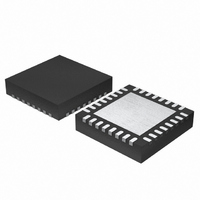
Manufacturer Part Number
DF38602RFT10
Description
MCU 3V 16K 32-QFN
Manufacturer
Renesas Electronics America
Series
H8® H8/300H SLPr
Datasheet
1.DF38602RFT10.pdf
(554 pages)
Specifications of DF38602RFT10
Core Processor
H8/300H
Core Size
16-Bit
Speed
10MHz
Connectivity
I²C, IrDA, SCI, SSU
Peripherals
POR, PWM, WDT
Number Of I /o
13
Program Memory Size
16KB (16K x 8)
Program Memory Type
FLASH
Ram Size
1K x 8
Voltage - Supply (vcc/vdd)
2.7 V ~ 3.6 V
Data Converters
A/D 6x10b
Oscillator Type
Internal
Operating Temperature
-20°C ~ 75°C
Package / Case
32-QFN
Lead Free Status / RoHS Status
Contains lead / RoHS non-compliant
Eeprom Size
-
Other names
HD64F38602RFT10
HD64F38602RFT10
HD64F38602RFT10
Available stocks
Company
Part Number
Manufacturer
Quantity
Price
Company:

Part Number:
DF38602RFT10V
Manufacturer:
Renesas Electronics America
Quantity:
135


Table 14.3
Table 14.4
Table 14.5
Table 14.6
Table 14.6
Table 14.7
Table 14.8
Table 14.9
Table 14.10
Table 14.11
Table 14.12
Table 14.13
Table 14.14
Section 15 Synchronous Serial Communication Unit (SSU)
Table 15.1
Table 15.2
Table 15.3
Section 16 I
Table 16.1
Table 16.2
Table 16.3
Table 16.4
Section 17 A/D Converter
Table 17.1
Table 17.2
Section 18 Comparators
Table 18.1
Table 18.2
Section 21 Electrical Characteristics
Table 21.1
Table 21.2
Table 21.3
Table 21.4
Table 21.5
Table 21.6
Table 21.7
Table 21.8
2
C Bus Interface 2 (IIC2)
Examples of BRR Settings for Various Bit Rates
Relation between n and Clock .............................................................................. 248
Maximum Bit Rate for Each Frequency (Asynchronous Mode) .......................... 248
BRR Settings for Various Bit Rates (Clock Synchronous Mode) (1) ................... 249
BRR Settings for Various Bit Rates (Clock Synchronous Mode) (2) ................... 250
Relation between n and Clock .............................................................................. 250
Data Transfer Formats (Asynchronous Mode)...................................................... 255
SMR Settings and Corresponding Data Transfer Formats.................................... 256
Pin Configuration.................................................................................................. 284
Relationship between Communication Modes and Input/Output Pins.................. 296
Interrupt Requests ................................................................................................. 310
Pin Configuration.................................................................................................. 313
Transfer Rate ........................................................................................................ 316
Interrupt Requests ................................................................................................. 345
Time for Monitoring SCL..................................................................................... 346
Pin Configuration.................................................................................................. 350
Operating States of A/D Converter....................................................................... 354
Pin Configuration.................................................................................................. 362
Combination of CMR and CMLS Bits ................................................................. 364
Absolute Maximum Ratings ................................................................................. 385
DC Characteristics ................................................................................................ 393
Control Signal Timing .......................................................................................... 399
Serial Interface Timing ......................................................................................... 402
Synchronous Serial Communication Unit (SSU) Timing ..................................... 403
I
A/D Converter Characteristics .............................................................................. 405
Comparator Characteristics................................................................................... 407
SMR and SCR Settings and Clock Source Selection............................................ 257
SSR Status Flags and Receive Data Handling...................................................... 262
IrCKS2 to IrCKS0 Bit Settings............................................................................. 273
SCI3 Interrupt Requests........................................................................................ 274
(Asynchronous Mode and ABCS Bit is 1) (4)...................................................... 247
Transmit/Receive Interrupts ................................................................................. 275
2
C Bus Interface Timing ...................................................................................... 404
Rev. 3.00 May 15, 2007 Page xxxi of xxxii
Related parts for DF38602RFT10
Image
Part Number
Description
Manufacturer
Datasheet
Request
R

Part Number:
Description:
KIT STARTER FOR M16C/29
Manufacturer:
Renesas Electronics America
Datasheet:

Part Number:
Description:
KIT STARTER FOR R8C/2D
Manufacturer:
Renesas Electronics America
Datasheet:

Part Number:
Description:
R0K33062P STARTER KIT
Manufacturer:
Renesas Electronics America
Datasheet:

Part Number:
Description:
KIT STARTER FOR R8C/23 E8A
Manufacturer:
Renesas Electronics America
Datasheet:

Part Number:
Description:
KIT STARTER FOR R8C/25
Manufacturer:
Renesas Electronics America
Datasheet:

Part Number:
Description:
KIT STARTER H8S2456 SHARPE DSPLY
Manufacturer:
Renesas Electronics America
Datasheet:

Part Number:
Description:
KIT STARTER FOR R8C38C
Manufacturer:
Renesas Electronics America
Datasheet:

Part Number:
Description:
KIT STARTER FOR R8C35C
Manufacturer:
Renesas Electronics America
Datasheet:

Part Number:
Description:
KIT STARTER FOR R8CL3AC+LCD APPS
Manufacturer:
Renesas Electronics America
Datasheet:
Part Number:
Description:
KIT STARTER FOR RX610
Manufacturer:
Renesas Electronics America
Datasheet:

Part Number:
Description:
KIT STARTER FOR R32C/118
Manufacturer:
Renesas Electronics America
Datasheet:

Part Number:
Description:
KIT DEV RSK-R8C/26-29
Manufacturer:
Renesas Electronics America
Datasheet:

Part Number:
Description:
KIT STARTER FOR SH7124
Manufacturer:
Renesas Electronics America
Datasheet:

Part Number:
Description:
KIT STARTER FOR H8SX/1622
Manufacturer:
Renesas Electronics America
Datasheet:

Part Number:
Description:
KIT DEV FOR SH7203
Manufacturer:
Renesas Electronics America
Datasheet: