DF38602RFT10 Renesas Electronics America, DF38602RFT10 Datasheet - Page 341
DF38602RFT10
Manufacturer Part Number
DF38602RFT10
Description
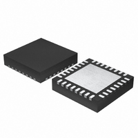
MCU 3V 16K 32-QFN
Manufacturer
Renesas Electronics America
Series
H8® H8/300H SLPr
Datasheet
1.DF38602RFT10.pdf
(554 pages)
Specifications of DF38602RFT10
Core Processor
H8/300H
Core Size
16-Bit
Speed
10MHz
Connectivity
I²C, IrDA, SCI, SSU
Peripherals
POR, PWM, WDT
Number Of I /o
13
Program Memory Size
16KB (16K x 8)
Program Memory Type
FLASH
Ram Size
1K x 8
Voltage - Supply (vcc/vdd)
2.7 V ~ 3.6 V
Data Converters
A/D 6x10b
Oscillator Type
Internal
Operating Temperature
-20°C ~ 75°C
Package / Case
32-QFN
Lead Free Status / RoHS Status
Contains lead / RoHS non-compliant
Eeprom Size
-
Other names
HD64F38602RFT10
HD64F38602RFT10
HD64F38602RFT10
Available stocks
Company
Part Number
Manufacturer
Quantity
Price
Company:

Part Number:
DF38602RFT10V
Manufacturer:
Renesas Electronics America
Quantity:
135


Section 15 Synchronous Serial Communication Unit (SSU)
15.4.9
Serial Data Reception
Figure 15.12 shows an example of the SSU operation for reception. In serial reception, the SSU
operates as described below.
When the SSU is set as a master device, it outputs a synchronous clock and inputs data. When the
SSU is set as a slave device, the SCS pin is in the low-input state and inputs data in synchronized
with the input clock. When the SSU is set as a master device, it outputs a receive clock and starts
reception by performing dummy read on SSRDR.
After eight bits of data is received, the RDRF bit in SSSR is set to 1 and received data is stored in
SSRDR. If the RIE bit in SSER is set to 1 at this time, an RXI is generated. If SSRDR is read, the
RDRF bit is automatically cleared to 0.
When the SSU is set as a master device and reception is ended, received data is read after setting
the RSSTP bit in SSER to 1. Then the SSU outputs eight bits of clocks and operation is stopped.
After that, the RE and RSSTP bits are cleared to 0 and the last received data is read. Note that if
SSRDR is read while the RE bit is set to 1, received clock is output again.
When the eighth clock rises while the RDRF bit is 1, the ORER bit in SSSR is set. Then an
overrun error (OEI) is generated and operation is stopped. When the ORER bit in SSSR is set to 1,
reception cannot be performed. Therefore confirm that the ORER bit is cleared to 0 before
reception.
The set timings of the RDRF and ORER flags differ according to the CPHS setting. These timings
are shown in figure 15.12. When the CPHS bit is set to 1, the flag is set during the frame.
Therefore care should be taken at the end of reception.
The sample flowchart for serial data reception is the same as that in clocked synchronous
communication mode.
Rev. 3.00 May 15, 2007 Page 307 of 518
REJ09B0152-0300
Related parts for DF38602RFT10
Image
Part Number
Description
Manufacturer
Datasheet
Request
R

Part Number:
Description:
KIT STARTER FOR M16C/29
Manufacturer:
Renesas Electronics America
Datasheet:

Part Number:
Description:
KIT STARTER FOR R8C/2D
Manufacturer:
Renesas Electronics America
Datasheet:

Part Number:
Description:
R0K33062P STARTER KIT
Manufacturer:
Renesas Electronics America
Datasheet:

Part Number:
Description:
KIT STARTER FOR R8C/23 E8A
Manufacturer:
Renesas Electronics America
Datasheet:

Part Number:
Description:
KIT STARTER FOR R8C/25
Manufacturer:
Renesas Electronics America
Datasheet:

Part Number:
Description:
KIT STARTER H8S2456 SHARPE DSPLY
Manufacturer:
Renesas Electronics America
Datasheet:

Part Number:
Description:
KIT STARTER FOR R8C38C
Manufacturer:
Renesas Electronics America
Datasheet:

Part Number:
Description:
KIT STARTER FOR R8C35C
Manufacturer:
Renesas Electronics America
Datasheet:

Part Number:
Description:
KIT STARTER FOR R8CL3AC+LCD APPS
Manufacturer:
Renesas Electronics America
Datasheet:
Part Number:
Description:
KIT STARTER FOR RX610
Manufacturer:
Renesas Electronics America
Datasheet:

Part Number:
Description:
KIT STARTER FOR R32C/118
Manufacturer:
Renesas Electronics America
Datasheet:

Part Number:
Description:
KIT DEV RSK-R8C/26-29
Manufacturer:
Renesas Electronics America
Datasheet:

Part Number:
Description:
KIT STARTER FOR SH7124
Manufacturer:
Renesas Electronics America
Datasheet:

Part Number:
Description:
KIT STARTER FOR H8SX/1622
Manufacturer:
Renesas Electronics America
Datasheet:

Part Number:
Description:
KIT DEV FOR SH7203
Manufacturer:
Renesas Electronics America
Datasheet: