MOD5272-100IR NetBurner Inc, MOD5272-100IR Datasheet - Page 489
MOD5272-100IR
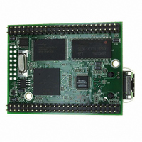
Manufacturer Part Number
MOD5272-100IR
Description
PROCESSOR MODULE FLASH MOD5272
Manufacturer
NetBurner Inc
Type
Controllers & Processorsr
Datasheets
1.MOD5272-100IR.pdf
(2 pages)
2.MOD5272-100IR.pdf
(3 pages)
3.MOD5272-100IR.pdf
(550 pages)
Specifications of MOD5272-100IR
Module/board Type
Processor Module
Ethernet Connection Type
10/100 Ethernet Port RJ-45
Operating Voltage
3.3 V
Product
Modules
Lead Free Status / RoHS Status
Lead free / RoHS Compliant
For Use With/related Products
MOD5272
For Use With
528-1001 - KIT DEVELOP NETWORK FOR MOD5272
Lead Free Status / Rohs Status
Lead free / RoHS Compliant
Other names
528-1008


MOTOROLA
21.5 Instruction Register
The MCF5272 IEEE 1149.1 implementation includes the three mandatory public
instructions (EXTEST, SAMPLE/PRELOAD, and BYPASS), the optional public ID
instruction, plus two additional public instructions (CLAMP and HI-Z) defined by IEEE
1149.1. The MCF5272 includes a 4-bit instruction register without parity, consisting of a
shift register with four parallel outputs. Data is transferred from the shift register to the
parallel outputs during the update-IR controller state. The 4 bits are used to decode the
instructions in Table 21-2.
The parallel output of the instruction register is reset to 0001 in the test-logic-reset
controller state. Note that this preset state is equivalent to the ID instruction.
B[3:0] Instruction
0000
0001
EXTEST
ID
NOTE: More than one lO.Cell could be serially connected and controlled by a single En.Cell.
Figure 21-7. General Arrangement for Bidirectional Pins
INPUT
The external test (EXTEST) instruction selects the boundary scan register. EXTEST asserts
internal reset for the MCF5272 system logic to force a predictable benign internal state while
performing external boundary scan operations.
By using the TAP, the register is capable of a) scanning user-defined values into the output
buffers, b) capturing values presented to input pins, c) controlling the direction of bidirectional
pins, and d) controlling the output drive of three-state output pins. For more details on the
function and uses of EXTEST, please refer to the IEEE 1149.1 document.
During the capture-IR controller state, the parallel inputs to the instruction shift register are
loaded with the 4-bit binary value (0001). The parallel outputs, however, remain unchanged
by this action since an update-IR signal is required to modify them.
DATA
O
E
O
Chapter 21. IEEE 1149.1 Test Access Port (JTAG)
FROM LAST CEL
Table 21-2. Instructions
TO NEXT CEL
EN.CELL
IO.CELL
*
*
DIRECTION
Description
OUTPUT
ENABLE
Instruction Register
I/O
PIN
21-7
Related parts for MOD5272-100IR
Image
Part Number
Description
Manufacturer
Datasheet
Request
R

Part Number:
Description:
Ethernet Modules & Development Tools MOD5272 Processor Board
Manufacturer:
NetBurner Inc
Datasheet:
Part Number:
Description:
Ethernet Modules & Development Tools MOD5272 Industrial Temperature
Manufacturer:
NetBurner Inc
Part Number:
Description:
Ethernet Modules & Development Tools MOD5272 MODULE
Manufacturer:
NetBurner Inc
Datasheet:

Part Number:
Description:
PROCESSOR MODULE FLASH
Manufacturer:
NetBurner Inc
Datasheet:

Part Number:
Description:
Ethernet Modules & Development Tools 32Bit 62MHz Core Module 50Pin DIP
Manufacturer:
NetBurner Inc
Datasheet:

Part Number:
Description:
BOARD SERIAL-ETHERNET 512K FLASH
Manufacturer:
NetBurner Inc
Datasheet:

Part Number:
Description:
PROCESSOR MODULE 512KB FLASH
Manufacturer:
NetBurner Inc
Datasheet:

Part Number:
Description:
DUAL PORT SERIAL-ETHERNET
Manufacturer:
NetBurner Inc
Datasheet:

Part Number:
Description:
PROCESSOR MODULE 512KB FLASH
Manufacturer:
NetBurner Inc
Datasheet:

Part Number:
Description:
MOD5234 10/100 ETHERNET MODULE
Manufacturer:
NetBurner Inc
Datasheet:

Part Number:
Description:
KIT DEVELOP NETWORK FOR MOD5282
Manufacturer:
NetBurner Inc
Datasheet:

Part Number:
Description:
KIT DEVELOP NETWORK FOR MOD5272
Manufacturer:
NetBurner Inc
Datasheet:

Part Number:
Description:
Ethernet ICs 32bit 147MHz CAN-to- Ethnt Device IndTemp
Manufacturer:
NetBurner Inc
Datasheet: