MOD5272-100IR NetBurner Inc, MOD5272-100IR Datasheet - Page 191
MOD5272-100IR
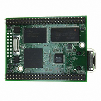
Manufacturer Part Number
MOD5272-100IR
Description
PROCESSOR MODULE FLASH MOD5272
Manufacturer
NetBurner Inc
Type
Controllers & Processorsr
Datasheets
1.MOD5272-100IR.pdf
(2 pages)
2.MOD5272-100IR.pdf
(3 pages)
3.MOD5272-100IR.pdf
(550 pages)
Specifications of MOD5272-100IR
Module/board Type
Processor Module
Ethernet Connection Type
10/100 Ethernet Port RJ-45
Operating Voltage
3.3 V
Product
Modules
Lead Free Status / RoHS Status
Lead free / RoHS Compliant
For Use With/related Products
MOD5272
For Use With
528-1001 - KIT DEVELOP NETWORK FOR MOD5272
Lead Free Status / Rohs Status
Lead free / RoHS Compliant
Other names
528-1008


MOTOROLA
8.2.1 Chip Select Base Registers (CSBR0–CSBR7)
The CSBRs, Figure 8-1, provide a model internal bus cycle against which to match actual
bus cycles to determine whether a specific chip select should assert. A bus cycle in a specific
chip select register causes the assertion of the corresponding external chip select.
Table 8-2 describes CSBRn fields.
Reset
31–12
11–10
Field
Addr
R/W
Bits
9–8
6–5
7
31
SUPER
Name
EBI
BW
BA
TT
CSBR0: 0x0000_0x01
CSBR4: 0x0000_4300; CSBR5: 0x0000_5300; CSBR6: 0x0000_6300; CSBR7: 0x0000_7700
Base address. The starting address of the memory space covered by the chip select. BA is
compared with bits 31–12 of the access to determine whether the current bus cycle is intended
for this chip select. Any combination of BA bits can be masked in the associated CSOR.
External bus interface modes. These modes are used to multiplex outputs and determine timing
of the appropriate bus interface module onto the device pins.
00 16-/32-bit SRAM/ROM. For 16-/32-bit wide memory devices with byte strobe inputs.
01 SDRAM. One physical bank of SDRAM consisting of 16–256 Mbit devices. CSOR7[WS] must
10 Reserved
11 Use SRAM/ROM timing for 8-bit devices without byte strobe inputs.
Bus width. Determines data bus size of the memory-mapped resource for all chip selects except
CS0. It is assumed that boot code for the processor is accessed through the global chip select
CS0, so the initial bus width for this chip select must be configured at reset. QSPI_CS0/BUSW0
and QSPI_CLK/BUSW1 are used to program the bus width for CS0 at reset.
00 Longword (32 bits)
01 Byte (8 bits)
10 Word (16 bits)
11 Cache line (32 bits)
Supervisor mode.
0 Bus cycle may be in user or supervisor mode (neglecting conditions imposed by setting CTM).
1 The chip select asserts a match only if the transfer modifier indicates a supervisor mode
SUPER, CTM, TT, and TM are used to restrict bus access. For example, if TT and TM indicate a
user data access and SUPER and CTM are both set, no accesses can occur.
Transfer type. TT and TM may be used to further qualify the address match. If CTM is set, TT and
TM must match the access types for the chip select to assert. See the description of TM.
BA
access. A user access matching BA causes an access error.
CSBR0[EBI] = 00 at reset. Affects all chip selects.
be set to 0x1F. Affects only CS7/SDCS.
Figure 8-1. Chip Select Base Registers (CSBRn)
0x040 (CSBR0); 0x048 (CSBR1); 0x050 (CSBR2); 0x058 (CSBR3);
0x060 (CSBR4); 0x068 (CSBR5); 0x070 (CSBR6); 0x078 (CSBR7)
Table 8-2. CSBRn Field Descriptions
12 11
1
; CSBR1: 0x0000_1300; CSBR2: 0x0000_2300; CSBR3: 0x0000_3300;
Chapter 8. Chip Select Module
EBI
10
9
BW
8
SUPER
R/W
Description
7
6
TT
5
4
TM
Chip Select Registers
2
CTM ENABLE
1
0
8-3
Related parts for MOD5272-100IR
Image
Part Number
Description
Manufacturer
Datasheet
Request
R

Part Number:
Description:
Ethernet Modules & Development Tools MOD5272 Processor Board
Manufacturer:
NetBurner Inc
Datasheet:
Part Number:
Description:
Ethernet Modules & Development Tools MOD5272 Industrial Temperature
Manufacturer:
NetBurner Inc
Part Number:
Description:
Ethernet Modules & Development Tools MOD5272 MODULE
Manufacturer:
NetBurner Inc
Datasheet:

Part Number:
Description:
PROCESSOR MODULE FLASH
Manufacturer:
NetBurner Inc
Datasheet:

Part Number:
Description:
Ethernet Modules & Development Tools 32Bit 62MHz Core Module 50Pin DIP
Manufacturer:
NetBurner Inc
Datasheet:

Part Number:
Description:
BOARD SERIAL-ETHERNET 512K FLASH
Manufacturer:
NetBurner Inc
Datasheet:

Part Number:
Description:
PROCESSOR MODULE 512KB FLASH
Manufacturer:
NetBurner Inc
Datasheet:

Part Number:
Description:
DUAL PORT SERIAL-ETHERNET
Manufacturer:
NetBurner Inc
Datasheet:

Part Number:
Description:
PROCESSOR MODULE 512KB FLASH
Manufacturer:
NetBurner Inc
Datasheet:

Part Number:
Description:
MOD5234 10/100 ETHERNET MODULE
Manufacturer:
NetBurner Inc
Datasheet:

Part Number:
Description:
KIT DEVELOP NETWORK FOR MOD5282
Manufacturer:
NetBurner Inc
Datasheet:

Part Number:
Description:
KIT DEVELOP NETWORK FOR MOD5272
Manufacturer:
NetBurner Inc
Datasheet:

Part Number:
Description:
Ethernet ICs 32bit 147MHz CAN-to- Ethnt Device IndTemp
Manufacturer:
NetBurner Inc
Datasheet: