MOD5272-100IR NetBurner Inc, MOD5272-100IR Datasheet - Page 210
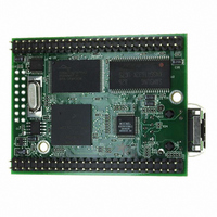
MOD5272-100IR
Manufacturer Part Number
MOD5272-100IR
Description
PROCESSOR MODULE FLASH MOD5272
Manufacturer
NetBurner Inc
Type
Controllers & Processorsr
Datasheets
1.MOD5272-100IR.pdf
(2 pages)
2.MOD5272-100IR.pdf
(3 pages)
3.MOD5272-100IR.pdf
(550 pages)
Specifications of MOD5272-100IR
Module/board Type
Processor Module
Ethernet Connection Type
10/100 Ethernet Port RJ-45
Operating Voltage
3.3 V
Product
Modules
Lead Free Status / RoHS Status
Lead free / RoHS Compliant
For Use With/related Products
MOD5272
For Use With
528-1001 - KIT DEVELOP NETWORK FOR MOD5272
Lead Free Status / Rohs Status
Lead free / RoHS Compliant
Other names
528-1008


SDRAM Interface
These SDRAM accesses are shown in Figure 9-9 through Figure 9-15. The SDRAM
supports a low-power, self-refreshing sleep mode as shown in Figure 9-14 and Figure 9-15.
It is also possible to turn off the SDRAM controller completely using the power
management control register in the SIM.
Figures show burst read and burst writes, with a page miss and a page hit for each case. A
single-cycle read or write is identical to the first access of a burst. In normal operation the
SDRAM controller refreshes the SDRAM.
As these examples show, SDCLKE is normally high and SDCLK is always active.
SDCLKE can be forced to 0 and SDCLK can be shut off by putting the SDRAM controller
into power down or self-refresh mode.
9.10.1 SDRAM Read Accesses
The read examples, Figure 9-9 and Figure 9-10, show a CAS latency of 2, SDCR[REG] = 0
and SDCR[INV] = 1.
In T1, the ColdFire core issues the address. This cycle is internal to the device and always
occurs. In T2, the SDRAM controller determines if there is a page miss or hit. This cycle is
internal to the device and always occurs.
Because Figure 9-9 shows a page miss, the
cycle occur. During precharge the SDRAM writes the designated on-chip RAM page buffer
back into the SDRAM array. The number of cycles for a precharge is set by programming
SDTR[RP]. The default after reset is two cycles. The activate new page cycle that follows
(T5) is required to open a new page due to the page miss. Cycle T6 is a wait state for
SDRAM activation command. It is added due to default value of 0b01 in SDTR[RCD]. For
lower clock speed systems the RCD value could be written as 00 and this clock cycle can
be removed. Consult the data sheets of the SDRAM devices being used.
9-16
• 16-byte cache line read bursts from 16-bit wide SDRAM with access times of
• 16-byte read or write bursts during Ethernet DMA transfers to/from SDRAM with
n-1-1-1-1-1-1-1. CSOR7[EXTBURST] must be set, CSBR7[EBI] must be set for
SDRAM, and CSBR7[BW] must be set for 16 bits.
access times of n-1-1-1 or n-1-1-1-1-1-1-1 depending on 32 or 16 bit SDRAM port
width as described in the previous two paragraphs.
MCF5272 User’s Manual
PRECHARGE
command (T3) and the following
MOTOROLA
Related parts for MOD5272-100IR
Image
Part Number
Description
Manufacturer
Datasheet
Request
R

Part Number:
Description:
Ethernet Modules & Development Tools MOD5272 Processor Board
Manufacturer:
NetBurner Inc
Datasheet:
Part Number:
Description:
Ethernet Modules & Development Tools MOD5272 Industrial Temperature
Manufacturer:
NetBurner Inc
Part Number:
Description:
Ethernet Modules & Development Tools MOD5272 MODULE
Manufacturer:
NetBurner Inc
Datasheet:

Part Number:
Description:
PROCESSOR MODULE FLASH
Manufacturer:
NetBurner Inc
Datasheet:

Part Number:
Description:
Ethernet Modules & Development Tools 32Bit 62MHz Core Module 50Pin DIP
Manufacturer:
NetBurner Inc
Datasheet:

Part Number:
Description:
BOARD SERIAL-ETHERNET 512K FLASH
Manufacturer:
NetBurner Inc
Datasheet:

Part Number:
Description:
PROCESSOR MODULE 512KB FLASH
Manufacturer:
NetBurner Inc
Datasheet:

Part Number:
Description:
DUAL PORT SERIAL-ETHERNET
Manufacturer:
NetBurner Inc
Datasheet:

Part Number:
Description:
PROCESSOR MODULE 512KB FLASH
Manufacturer:
NetBurner Inc
Datasheet:

Part Number:
Description:
MOD5234 10/100 ETHERNET MODULE
Manufacturer:
NetBurner Inc
Datasheet:

Part Number:
Description:
KIT DEVELOP NETWORK FOR MOD5282
Manufacturer:
NetBurner Inc
Datasheet:

Part Number:
Description:
KIT DEVELOP NETWORK FOR MOD5272
Manufacturer:
NetBurner Inc
Datasheet:

Part Number:
Description:
Ethernet ICs 32bit 147MHz CAN-to- Ethnt Device IndTemp
Manufacturer:
NetBurner Inc
Datasheet: