MOD5272-100IR NetBurner Inc, MOD5272-100IR Datasheet - Page 435
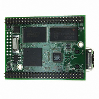
MOD5272-100IR
Manufacturer Part Number
MOD5272-100IR
Description
PROCESSOR MODULE FLASH MOD5272
Manufacturer
NetBurner Inc
Type
Controllers & Processorsr
Datasheets
1.MOD5272-100IR.pdf
(2 pages)
2.MOD5272-100IR.pdf
(3 pages)
3.MOD5272-100IR.pdf
(550 pages)
Specifications of MOD5272-100IR
Module/board Type
Processor Module
Ethernet Connection Type
10/100 Ethernet Port RJ-45
Operating Voltage
3.3 V
Product
Modules
Lead Free Status / RoHS Status
Lead free / RoHS Compliant
For Use With/related Products
MOD5272
For Use With
528-1001 - KIT DEVELOP NETWORK FOR MOD5272
Lead Free Status / Rohs Status
Lead free / RoHS Compliant
Other names
528-1008


MOTOROLA
19.6.3 Read/Write (R/W)
R/W is programmed on a per-chip-select basis for use with SRAM and external peripheral
write accesses. It should be connected to the external peripheral or memory write enable
signal.
R/W acts as a write strobe to external SRAM when the decoded chip select is configured
for either of the two SRAM/ROM modes. It is asserted during on-chip peripherals accesses
and negated during on-chip SRAM accesses.
19.6.4 Transfer Acknowledge (TA/PB5)
Assertion of the transfer acknowledge (TA/PB5) input terminates an external bus cycle. It
is enabled on a per chip select basis by programming the wait state field to 0x1F in the
corresponding chip select option register (CSORn[WS]). This pin requires a 4.7-KΩ
pull-up resistor or external logic that drives inactive high.
TA must always be returned high before it can be detected again. Asserting TA into the next
bus cycle has no effect and does not terminate the bus cycle.
19.6.5 Hi-Z
HiZ is a test signal. When it is connected to GND during reset, all output pins are driven to
high impedance. A 4.7-KΩ pullup resistor should be connected to this signal if the Hi-Z
function is not used. Hi-Z configuration input is sampled on the rising edge of Reset Output
(RSTO).
Even though EBI modes set to SDRAM require setting the wait
state field in the chip select option register to 31, a low signal
should never be applied to TA during such accesses. For
SDRAM accesses the bus cycle is terminated internally by
circuitry in the SDRAM module.
16 Bit 32 Bit
BS3
BS2
NC
NC
5272
Table 19-6. Connecting BS[3:0] to DQMx
BS3
BS2
BS1
BS0
DQMH
DQML
16 Bit
Chapter 19. Signal Descriptions
NC
NC
32 Bit (2 x 16) 32 Bit (1 x 32)
DQMH
DQMH
DQML
DQML
NOTE:
SDRAM
DQM3
DQM2
DQM1
DQM0
Data Signals
D[31:24]
D[23:16]
D[15:8]
D[7:0]
Bus Control Signals
19-21
Related parts for MOD5272-100IR
Image
Part Number
Description
Manufacturer
Datasheet
Request
R

Part Number:
Description:
Ethernet Modules & Development Tools MOD5272 Processor Board
Manufacturer:
NetBurner Inc
Datasheet:
Part Number:
Description:
Ethernet Modules & Development Tools MOD5272 Industrial Temperature
Manufacturer:
NetBurner Inc
Part Number:
Description:
Ethernet Modules & Development Tools MOD5272 MODULE
Manufacturer:
NetBurner Inc
Datasheet:

Part Number:
Description:
PROCESSOR MODULE FLASH
Manufacturer:
NetBurner Inc
Datasheet:

Part Number:
Description:
Ethernet Modules & Development Tools 32Bit 62MHz Core Module 50Pin DIP
Manufacturer:
NetBurner Inc
Datasheet:

Part Number:
Description:
BOARD SERIAL-ETHERNET 512K FLASH
Manufacturer:
NetBurner Inc
Datasheet:

Part Number:
Description:
PROCESSOR MODULE 512KB FLASH
Manufacturer:
NetBurner Inc
Datasheet:

Part Number:
Description:
DUAL PORT SERIAL-ETHERNET
Manufacturer:
NetBurner Inc
Datasheet:

Part Number:
Description:
PROCESSOR MODULE 512KB FLASH
Manufacturer:
NetBurner Inc
Datasheet:

Part Number:
Description:
MOD5234 10/100 ETHERNET MODULE
Manufacturer:
NetBurner Inc
Datasheet:

Part Number:
Description:
KIT DEVELOP NETWORK FOR MOD5282
Manufacturer:
NetBurner Inc
Datasheet:

Part Number:
Description:
KIT DEVELOP NETWORK FOR MOD5272
Manufacturer:
NetBurner Inc
Datasheet:

Part Number:
Description:
Ethernet ICs 32bit 147MHz CAN-to- Ethnt Device IndTemp
Manufacturer:
NetBurner Inc
Datasheet: