MOD5272-100IR NetBurner Inc, MOD5272-100IR Datasheet - Page 209
MOD5272-100IR
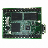
Manufacturer Part Number
MOD5272-100IR
Description
PROCESSOR MODULE FLASH MOD5272
Manufacturer
NetBurner Inc
Type
Controllers & Processorsr
Datasheets
1.MOD5272-100IR.pdf
(2 pages)
2.MOD5272-100IR.pdf
(3 pages)
3.MOD5272-100IR.pdf
(550 pages)
Specifications of MOD5272-100IR
Module/board Type
Processor Module
Ethernet Connection Type
10/100 Ethernet Port RJ-45
Operating Voltage
3.3 V
Product
Modules
Lead Free Status / RoHS Status
Lead free / RoHS Compliant
For Use With/related Products
MOD5272
For Use With
528-1001 - KIT DEVELOP NETWORK FOR MOD5272
Lead Free Status / Rohs Status
Lead free / RoHS Compliant
Other names
528-1008


MOTOROLA
9.10 SDRAM Interface
Setting CSBRn[EBI] to 0b01 enables chip select CS7 for use with one physical bank of
SDRAM. In this case, CS7 becomes SDCS. The SDRAM memory array may have a 32- or
16-bit data bus width; an 8-bit width is not supported. An array may consist of SDRAM
devices with 8, 16, or 32 bits data bus width. Each SDRAM device can have from 16–256
Mbits.
The interface to the SDRAM devices is glueless. The following control signals are
dedicated to SDRAM: SDCS, SDWE, A10_PRECHG, SDCLK, SDCLKE, RAS0, CAS0,
and SDBA[1:0].
If SDRAM EBI mode is used, CSOR7[WAITST] should be programmed for 0x1F to
ensure that the internal bus cycle termination signal is sourced from the SDRAM controller
and not the chip select module.
The controller allows single-beat read/write accesses and the following burst accesses:
• 16-byte cache line read bursts from 32-bit wide SDRAM with access times of
n-1-1-1. The value of n depends on read, write, page miss, page hit, etc. The enable
extended bursts bit in chip select option register 7 (CSOR7[EXTBURST]) must be
cleared, CSBR7[EBI] must be set for SDRAM, and CSBR7[BW] must be set for a
16-byte cache line width.
When reduced effective CAS latency is used, the SDRAM is
still programmed with true CAS latency. The SDRAM
controller state machine must be reprogrammed for the
reduced CAS latency. SDRAM initialization software
programs the CAS latency of 2 and transfers it into the
SDRAM mode register. After SDRAM initialization is
confirmed, initialization software should change SDTR[CLT]
to CAS latency 1 but should not reinitialize the SDRAM. The
SDRAM controller state machine now runs with CAS latency
1 and SDRAMs run with CAS latency 2, which increases
bandwidth on the SDRAM bank and improves performance.
The SDRAM shares address and data signals with external
memory and peripherals. Due to stringent SDRAM timing
requirements, it is strongly recommended to buffer the address,
byte strobe, and data buses between the MCF5272 and
non-SDRAM memory and peripherals. Never buffer signals to
the SDRAMs. See Appendix C for details on how to buffer
external memory and peripherals in a system using SDRAM.
Chapter 9. SDRAM Controller
NOTE:
NOTE:
SDRAM Interface
9-15
Related parts for MOD5272-100IR
Image
Part Number
Description
Manufacturer
Datasheet
Request
R

Part Number:
Description:
Ethernet Modules & Development Tools MOD5272 Processor Board
Manufacturer:
NetBurner Inc
Datasheet:
Part Number:
Description:
Ethernet Modules & Development Tools MOD5272 Industrial Temperature
Manufacturer:
NetBurner Inc
Part Number:
Description:
Ethernet Modules & Development Tools MOD5272 MODULE
Manufacturer:
NetBurner Inc
Datasheet:

Part Number:
Description:
PROCESSOR MODULE FLASH
Manufacturer:
NetBurner Inc
Datasheet:

Part Number:
Description:
Ethernet Modules & Development Tools 32Bit 62MHz Core Module 50Pin DIP
Manufacturer:
NetBurner Inc
Datasheet:

Part Number:
Description:
BOARD SERIAL-ETHERNET 512K FLASH
Manufacturer:
NetBurner Inc
Datasheet:

Part Number:
Description:
PROCESSOR MODULE 512KB FLASH
Manufacturer:
NetBurner Inc
Datasheet:

Part Number:
Description:
DUAL PORT SERIAL-ETHERNET
Manufacturer:
NetBurner Inc
Datasheet:

Part Number:
Description:
PROCESSOR MODULE 512KB FLASH
Manufacturer:
NetBurner Inc
Datasheet:

Part Number:
Description:
MOD5234 10/100 ETHERNET MODULE
Manufacturer:
NetBurner Inc
Datasheet:

Part Number:
Description:
KIT DEVELOP NETWORK FOR MOD5282
Manufacturer:
NetBurner Inc
Datasheet:

Part Number:
Description:
KIT DEVELOP NETWORK FOR MOD5272
Manufacturer:
NetBurner Inc
Datasheet:

Part Number:
Description:
Ethernet ICs 32bit 147MHz CAN-to- Ethnt Device IndTemp
Manufacturer:
NetBurner Inc
Datasheet: