MOD5272-100IR NetBurner Inc, MOD5272-100IR Datasheet - Page 200
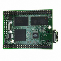
MOD5272-100IR
Manufacturer Part Number
MOD5272-100IR
Description
PROCESSOR MODULE FLASH MOD5272
Manufacturer
NetBurner Inc
Type
Controllers & Processorsr
Datasheets
1.MOD5272-100IR.pdf
(2 pages)
2.MOD5272-100IR.pdf
(3 pages)
3.MOD5272-100IR.pdf
(550 pages)
Specifications of MOD5272-100IR
Module/board Type
Processor Module
Ethernet Connection Type
10/100 Ethernet Port RJ-45
Operating Voltage
3.3 V
Product
Modules
Lead Free Status / RoHS Status
Lead free / RoHS Compliant
For Use With/related Products
MOD5272
For Use With
528-1001 - KIT DEVELOP NETWORK FOR MOD5272
Lead Free Status / Rohs Status
Lead free / RoHS Compliant
Other names
528-1008


SDRAM Banks, Page Hits, and Page Misses
9.4 SDRAM Banks, Page Hits, and Page Misses
SDRAMs can have up to four banks addressed by SDBA1 and SDBA0. The two uppermost
address lines of the memory space are mapped to SDBA1 and SDBA0. Specific address
lines mapped depend on the size of the SDRAM array and are defined in the SDCR.
Each of the four bank address registers holds the page address (lower bits of row address)
of an activated page. Each bank can have one open page. A device with two banks can have
two open pages. A device with four banks can have four open pages.
The lower addresses of the row address are compared against the page address register
content. If it does not match, the SDRAM controller precharges the open page on the
accessed bank and activates the new required page. After this, the SDRAM controller
executes the
is updated. This is called a page miss.
After a bank is activated, it remains activated until the next page access causing a page miss.
A precharge of a deactivated bank is allowed and simply ignored by the SDRAM.
If a memory access is to an open page only the
SDRAM. This is called a page hit.
In two-page SDRAMs, banks 2 and 3 are invalid and must not be addressed. To avoid
address aliasing, the user should restrict the chip select address range to the space available
in the SDRAMs.
9.5 SDRAM Registers
The SDRAM configuration register (SDCR) and the SDRAM timing register (SDTR) are
described in the following sections. Note that SDRAM provides a mode register that is not
part of the SDRAM controller memory model. The SDRAM mode register is automatically
configured during initialization.
9.5.1 SDRAM Configuration Register (SDCR)
SDCR is used to configure the SDRAM controller address multiplexers for the type of
SDRAM devices used on the system board.
9-6
Reset
Write
Addr
R/W
—
15
0
READ
14
MCAS
00
Figure 9-3. SDRAM Configuration Register (SDCR)
13
or
WRITE
12
00
—
command. Concurrently, the page address register of the bank
11
10
MCF5272 User’s Manual
Read/Write
BALOC
001
MBAR + 0x0182
8
READ
GSL
7
0
or
6
00
—
WRITE
5
REG
command is issued to the
4
0
INV SLEEP ACT
1
3
Read-only
2
0
MOTOROLA
0
1
INIT
R/W
0
0
Related parts for MOD5272-100IR
Image
Part Number
Description
Manufacturer
Datasheet
Request
R

Part Number:
Description:
Ethernet Modules & Development Tools MOD5272 Processor Board
Manufacturer:
NetBurner Inc
Datasheet:
Part Number:
Description:
Ethernet Modules & Development Tools MOD5272 Industrial Temperature
Manufacturer:
NetBurner Inc
Part Number:
Description:
Ethernet Modules & Development Tools MOD5272 MODULE
Manufacturer:
NetBurner Inc
Datasheet:

Part Number:
Description:
PROCESSOR MODULE FLASH
Manufacturer:
NetBurner Inc
Datasheet:

Part Number:
Description:
Ethernet Modules & Development Tools 32Bit 62MHz Core Module 50Pin DIP
Manufacturer:
NetBurner Inc
Datasheet:

Part Number:
Description:
BOARD SERIAL-ETHERNET 512K FLASH
Manufacturer:
NetBurner Inc
Datasheet:

Part Number:
Description:
PROCESSOR MODULE 512KB FLASH
Manufacturer:
NetBurner Inc
Datasheet:

Part Number:
Description:
DUAL PORT SERIAL-ETHERNET
Manufacturer:
NetBurner Inc
Datasheet:

Part Number:
Description:
PROCESSOR MODULE 512KB FLASH
Manufacturer:
NetBurner Inc
Datasheet:

Part Number:
Description:
MOD5234 10/100 ETHERNET MODULE
Manufacturer:
NetBurner Inc
Datasheet:

Part Number:
Description:
KIT DEVELOP NETWORK FOR MOD5282
Manufacturer:
NetBurner Inc
Datasheet:

Part Number:
Description:
KIT DEVELOP NETWORK FOR MOD5272
Manufacturer:
NetBurner Inc
Datasheet:

Part Number:
Description:
Ethernet ICs 32bit 147MHz CAN-to- Ethnt Device IndTemp
Manufacturer:
NetBurner Inc
Datasheet: