MOD5272-100IR NetBurner Inc, MOD5272-100IR Datasheet - Page 448
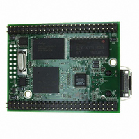
MOD5272-100IR
Manufacturer Part Number
MOD5272-100IR
Description
PROCESSOR MODULE FLASH MOD5272
Manufacturer
NetBurner Inc
Type
Controllers & Processorsr
Datasheets
1.MOD5272-100IR.pdf
(2 pages)
2.MOD5272-100IR.pdf
(3 pages)
3.MOD5272-100IR.pdf
(550 pages)
Specifications of MOD5272-100IR
Module/board Type
Processor Module
Ethernet Connection Type
10/100 Ethernet Port RJ-45
Operating Voltage
3.3 V
Product
Modules
Lead Free Status / RoHS Status
Lead free / RoHS Compliant
For Use With/related Products
MOD5272
For Use With
528-1001 - KIT DEVELOP NETWORK FOR MOD5272
Lead Free Status / Rohs Status
Lead free / RoHS Compliant
Other names
528-1008


Physical Layer Interface Controller TDM Ports and UART 1
19.16.2.3 GCI/IDL Data In (DIN1)
IDL mode: The DIN1 input is for clocking data into IDL port 1. Data is clocked into DIN1
on the falling edge of DCL1. DIN1 is also used for clocking data into ports 2 and 3.
GCI mode: The DIN1 input is for clocking data into GCI port 1. DCL1 is twice the bit rate,
that is, two clocks per data bit. DIN1 is also used for clocking data into ports 2 and 3.
19.16.2.4 GCI/IDL Frame Sync (FSC1/FSR1/DFSC1)
IDL mode: FSR1 is an input for the 8-KHz frame sync for port 1.
GCI mode: FSC1 is an input for the 8-KHz frame sync for port 1. Normally the GCI FSC
signal is two clocks wide and is aligned with the first B channel bit of the GCI frame. Many
U-interface devices including the MC145572 and MC145576 change the width of FSC to
one clock every 12 mS, indicating a U-interface super frame boundary. The MCF5272 can
accept either frame sync width.
When this pin is configured as an output, the DFSC1 sync signal from the on-chip clock
synthesizer is output on this pin. Also DFSC1 is used to internally drive the port 1 frame
sync and the delayed sync generators associated with ports 2 and 3. The width of DFSC1
can be configured for 1, 2, 8, or 16 DCL clocks duration. The location of DFSC1 is
programmable in single clock increments up to a maximum count of 0x3FF.
19.16.2.5 D-Channel Request (DREQ1/PA14)
IDL mode: This pin can be configured as the DREQ1 output in IDL mode for signalling to
a layer 1 S/T transceiver that a frame of data is ready to be sent on the port 1 D channel.
Port A mode: I/O pin PA14.
19.16.2.6 D-Channel Grant (DGNT1_INT6/PA15_INT6)
This pin can be independently configured as the input, DGNT1, used by a Layer one ISDN
S/T transceiver to indicate that D-channel access has been granted.
Port A mode: I/O pin PA15.
Special interrupt mode: The INT6 interrupt can be enabled independently of the pin being
configured for DGNT1 or PA15. This is particularly useful when configured for PA15
operation because INT6 can be used to signal a change of data on the PAx pins.
19.16.3 GCI/IDL TDM Ports 2 and 3
Physical Layer Interface port 2 is an additional GCI/IDL port. This Physical Layer Interface
shares the DIN1, DOUT1, and DCL1 pins of Physical Layer Interface port 1. The operating
mode is selected by the same register control bit that selects the operating mode for port 1.
19-34
MCF5272 User’s Manual
MOTOROLA
Related parts for MOD5272-100IR
Image
Part Number
Description
Manufacturer
Datasheet
Request
R

Part Number:
Description:
Ethernet Modules & Development Tools MOD5272 Processor Board
Manufacturer:
NetBurner Inc
Datasheet:
Part Number:
Description:
Ethernet Modules & Development Tools MOD5272 Industrial Temperature
Manufacturer:
NetBurner Inc
Part Number:
Description:
Ethernet Modules & Development Tools MOD5272 MODULE
Manufacturer:
NetBurner Inc
Datasheet:

Part Number:
Description:
PROCESSOR MODULE FLASH
Manufacturer:
NetBurner Inc
Datasheet:

Part Number:
Description:
Ethernet Modules & Development Tools 32Bit 62MHz Core Module 50Pin DIP
Manufacturer:
NetBurner Inc
Datasheet:

Part Number:
Description:
BOARD SERIAL-ETHERNET 512K FLASH
Manufacturer:
NetBurner Inc
Datasheet:

Part Number:
Description:
PROCESSOR MODULE 512KB FLASH
Manufacturer:
NetBurner Inc
Datasheet:

Part Number:
Description:
DUAL PORT SERIAL-ETHERNET
Manufacturer:
NetBurner Inc
Datasheet:

Part Number:
Description:
PROCESSOR MODULE 512KB FLASH
Manufacturer:
NetBurner Inc
Datasheet:

Part Number:
Description:
MOD5234 10/100 ETHERNET MODULE
Manufacturer:
NetBurner Inc
Datasheet:

Part Number:
Description:
KIT DEVELOP NETWORK FOR MOD5282
Manufacturer:
NetBurner Inc
Datasheet:

Part Number:
Description:
KIT DEVELOP NETWORK FOR MOD5272
Manufacturer:
NetBurner Inc
Datasheet:

Part Number:
Description:
Ethernet ICs 32bit 147MHz CAN-to- Ethnt Device IndTemp
Manufacturer:
NetBurner Inc
Datasheet: