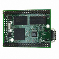
MOD5272-100IR NetBurner Inc, MOD5272-100IR Datasheet - Page 449
MOD5272-100IR
Manufacturer Part Number
MOD5272-100IR
Description
PROCESSOR MODULE FLASH MOD5272
Manufacturer
NetBurner Inc
Type
Controllers & Processorsr
Datasheets
1.MOD5272-100IR.pdf
(2 pages)
2.MOD5272-100IR.pdf
(3 pages)
3.MOD5272-100IR.pdf
(550 pages)
Specifications of MOD5272-100IR
Module/board Type
Processor Module
Ethernet Connection Type
10/100 Ethernet Port RJ-45
Operating Voltage
3.3 V
Product
Modules
Lead Free Status / RoHS Status
Lead free / RoHS Compliant
For Use With/related Products
MOD5272
For Use With
528-1001 - KIT DEVELOP NETWORK FOR MOD5272
Lead Free Status / Rohs Status
Lead free / RoHS Compliant
Other names
528-1008


Physical Layer Interface Controller TDM Ports and UART 1
Physical Layer Interface port 3 is an additional GCI/IDL port. This Physical Layer Interface
shares the DIN1, DOUT1, and DCL1 pins of Physical Layer Interface port 1. The operating
mode is selected by the same register control bit that selects the operating mode for port 1.
Port 3 can also have its input and output signals redirected to DIN3 and DOUT3
respectively.
19.16.3.1 GCI/IDL Delayed Frame Sync 2 (DFSC2/PA12)
IDL/GCI Modes: DFSC2 is used as a programmable delayed frame sync for external
IDL/GCI devices that use port 2 but are connected to the port 1 data pins. Port 2 uses the
DFSC2 frame sync internally to ensure alignment with external devices synchronized with
DFSC2. The width of this signal can be configured for 1, 2, 8, or 16 DCL clocks duration.
The location of this frame sync is programmable in single clock increments up to a
maximum count of 0x3FF.
Port A mode: I/O pin PA12.
19.16.3.2 GCI/IDL Delayed Frame Sync 3 (DFSC3/PA13)
Output pin DFSC3. This active high signal is used as a programmable delayed frame sync
for external IDL/GCI devices that use port 3 but are connected to the port 1 or port 3 data
pins. Port 3 uses the DFSC3 frame sync internally to ensure alignment with external devices
synchronized with DFSC3. The width of this signal can be configured for 1, 2, 8, or 16 DCL
clocks duration. The location of this frame sync is programmable in single clock increments
up to a maximum count of 0x3FF.
Port A mode: I/O pin PA13.
19.16.3.3 QSPI_CS3, Port 3 GCI/IDL Data Out 3, PA7
(PA7/DOUT3/QSPI_CS3)
QSPI mode: The QSPI chip select, QSPI_CS3, is the default configuration after device
reset. QSPI_CS3 can be programmed to be active high or low.
IDL mode: This pin can be configured as a dedicated output for clocking data out of IDL
port 3. Data is clocked out of DOUT3 on the rising edge of DCL1. After device reset port
3 is connected to DOUT1 by setting a bit in the PLIC module configuration register, this
pin can be configured as a dedicated output for IDL/GCI port 3.
GCI mode: This pin can be configured as a dedicated output for clocking data out of GCI
port 3. Data is clocked out of DOUT3 on the rising edge of DCL1. DCL1 is twice the bit
rate, that is, two clocks per data bit. This is done by setting a bit in the PLIC module
configuration register this pin can be configured as a dedicated output for IDL/GCI port 3.
Port A mode: I/O pin PA7.
MOTOROLA
Chapter 19. Signal Descriptions
19-35
Related parts for MOD5272-100IR
Image
Part Number
Description
Manufacturer
Datasheet
Request
R

Part Number:
Description:
Ethernet Modules & Development Tools MOD5272 Processor Board
Manufacturer:
NetBurner Inc
Datasheet:
Part Number:
Description:
Ethernet Modules & Development Tools MOD5272 Industrial Temperature
Manufacturer:
NetBurner Inc
Part Number:
Description:
Ethernet Modules & Development Tools MOD5272 MODULE
Manufacturer:
NetBurner Inc
Datasheet:

Part Number:
Description:
PROCESSOR MODULE FLASH
Manufacturer:
NetBurner Inc
Datasheet:

Part Number:
Description:
Ethernet Modules & Development Tools 32Bit 62MHz Core Module 50Pin DIP
Manufacturer:
NetBurner Inc
Datasheet:

Part Number:
Description:
BOARD SERIAL-ETHERNET 512K FLASH
Manufacturer:
NetBurner Inc
Datasheet:

Part Number:
Description:
PROCESSOR MODULE 512KB FLASH
Manufacturer:
NetBurner Inc
Datasheet:

Part Number:
Description:
DUAL PORT SERIAL-ETHERNET
Manufacturer:
NetBurner Inc
Datasheet:

Part Number:
Description:
PROCESSOR MODULE 512KB FLASH
Manufacturer:
NetBurner Inc
Datasheet:

Part Number:
Description:
MOD5234 10/100 ETHERNET MODULE
Manufacturer:
NetBurner Inc
Datasheet:

Part Number:
Description:
KIT DEVELOP NETWORK FOR MOD5282
Manufacturer:
NetBurner Inc
Datasheet:

Part Number:
Description:
KIT DEVELOP NETWORK FOR MOD5272
Manufacturer:
NetBurner Inc
Datasheet:

Part Number:
Description:
Ethernet ICs 32bit 147MHz CAN-to- Ethnt Device IndTemp
Manufacturer:
NetBurner Inc
Datasheet: